






















































 HOME


-

Ceramic PCB for Humanoid Robot joint actuators
2026 04,07 -
LTCC PCB Surprises: What Most People Miss
2025 12,09 -
Step-by-Step Guide to DPC PCB Design for Sensor Systems
2025 12,03 -
Ceramic PCBs Essential Benefits and Applications
2025 12,01 -
How Al2O3 DPC Ceramic Substrate PCB Enhances Heat Dissipation in Modern Electronics?
2025 11,28 -
How to Choose Between Ceramic, FR4, and Metal Core PCBs
2025 11,27 -
DPC Ceramic PCB Materials: Surprising Science Inside
2025 11,26 -
Wire bondable 2-layer Alumina substrates PCB | Bstceramic PCB
2025 09,22 -
Silicon Nitride Substrate, Silicon Nitride Ceramic Substrate Formula
2025 05,08 -
What is thick film ceramic PCB?
2023 08,02
What Is Moly Manganese Metallization in Ceramic Electronics?
Published:
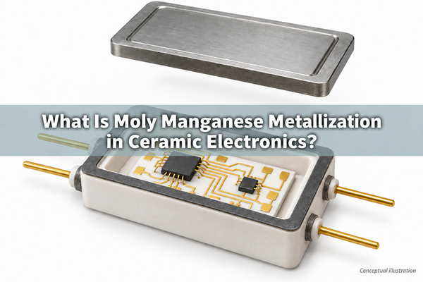
Moly manganese metallization forms a bonded metal-containing layer on ceramic so that a plated surface can subsequently be brazed to metal. In ceramic electronics, it is mainly associated with seal bands, feedthroughs and package connections. It is not another name for the copper traces on a ceramic PCB. The distinction matters when a design combines a ceramic circuit substrate with a metal enclosure or hermetic package.
What Is Moly Manganese Metallization?
Molybdenum manganese metallization, often shortened to Mo-Mn metallization, is a refractory thick-film process. A prepared paste is applied to selected ceramic surfaces and fired to establish adhesion. A subsequent metal finish, commonly nickel, provides a surface suitable for joining.
The fired layer contains a metallic network and an interfacial bonding system; it is not simply a sheet of molybdenum glued to alumina. Paste chemistry, the ceramic grade and the firing atmosphere work together. A continuous coating is useful, but continuity alone does not establish bond strength or a leak-tight joint.
How Is Mo-Mn Metallization Related to Ceramic PCBs?
Mo-Mn can provide the joining interface around a ceramic electronic assembly, while the ceramic PCB provides the circuit connections. These functions may be on separate parts or in separately specified regions of a package. They should not be treated as interchangeable manufacturing requirements.
For example, a ceramic circuit tile can carry die-attach pads and wire-bond pads inside a housing. A metallized ceramic frame can provide a joining surface around that housing. The tile needs defined conductor geometry and electrical performance; the frame needs a continuous seal path and a compatible joining process. A reliable circuit tile does not, by itself, make the enclosure hermetic.
At BSTCeramicPCB, we supply ceramic circuit boards. For an assembly that also includes a Mo-Mn seal, your drawing needs to distinguish the circuit substrate from the package and its joining surfaces. This keeps circuit fabrication requirements separate from ceramic-to-metal sealing requirements.
How Does the Moly Manganese Process Work?
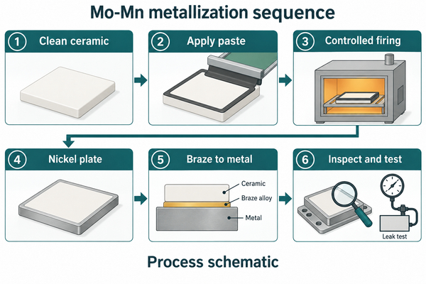
The moly manganese process normally follows surface preparation, paste application, controlled firing, finishing and joining. Metallization is completed before temperature-sensitive electronic components are assembled.
- Prepare the ceramic. Clean the surface and check the areas that will receive metallization. Edge damage or contamination at a narrow seal land can interrupt the eventual joint.
- Apply the paste. Screen printing suits many flat patterns; other deposition methods suit cylindrical bands or shaped parts. The drawing defines which surfaces must remain bare.
- Dry and fire. Remove the organic vehicle and fire using a qualified atmosphere and temperature profile. Published conventional processes operate around 1,500 degrees C, but the actual cycle depends on the ceramic and paste system.
- Apply the finish. Nickel plating is common after firing. Some process routes include an additional heat treatment before joining.
- Join and inspect. The prepared surface is brazed to the specified metal part, then evaluated against the joint's mechanical, electrical and leakage requirements.
The firing temperature is a manufacturing condition, not the operating-temperature rating of the completed PCB assembly. Components, solder, braze alloy and package construction impose separate limits.
Why Is Nickel Applied over the Mo-Mn Layer?
Nickel provides a practical wettable surface for subsequent joining and helps protect the fired metallization. The Mo-Mn layer and the nickel finish therefore have different jobs: the first establishes the ceramic-side interface; the second prepares the metal-facing surface.
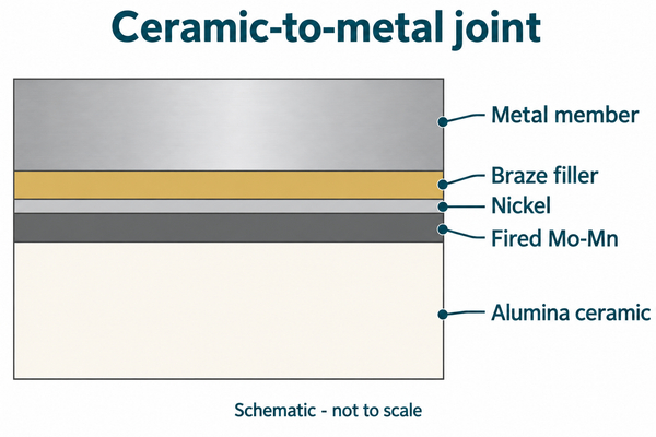
Do not combine both layers into a single unspecified "metal thickness" on a drawing. Identify the fired metallization, plated finish and thickness requirements separately. A coating-thickness measurement also needs the correct material model and calibration; a reading for nickel alone does not describe the full interface.
For circuit pads, the finish must also suit the intended attachment method. A finish selected for brazing a seal ring is not automatically the right finish for fine wire bonding or solder assembly elsewhere on the ceramic.
Which Ceramic Grades Can Use Mo-Mn Metallization?
Alumina is a common substrate for this process, but alumina grades are not interchangeable. The glass phase and other constituents influence how the fired layer bonds. High-purity alumina and sapphire can also be metallized using suitable formulations; they do not necessarily accept the same paste and firing cycle as a lower-purity grade.
Specify the material grade rather than only "white ceramic" or "Al2O3." For a ceramic PCB, electrical insulation, dielectric properties, surface condition and thermal requirements still matter. Increasing purity to satisfy an electrical requirement may also change the metallization process needed at a joining surface.
Metallized alumina is a description of a material with a metal layer, not a complete PCB specification. It does not establish conductor geometry, usable current, pad finish or whether the part has been qualified for hermetic sealing.
How Does Mo-Mn Differ from Ceramic Circuit Metallization?
The main distinction is what the metal layer must do. A seal land must support joining; a circuit pattern must route electrical connections. Metallization of ceramic substrates can serve either purpose, but the process and acceptance criteria follow the function.
| Process or structure | Main purpose in the design | What must be specified |
|---|---|---|
| Fired Mo-Mn with a plated finish | Joining selected ceramic surfaces to metal | Ceramic grade, coated region, finish, joint geometry and joining conditions |
| Thick-film ceramic circuit | Printed conductors and, where required, printed resistors | Paste system, conductor pattern, resistor requirements and firing compatibility |
| Thin-film ceramic circuit | Patterned deposited films for electronic interconnection or functional layers | Film stack, adhesion layer, pattern dimensions and pad finish |
| DPC ceramic circuit | Copper circuitry built over an adhesion/seed system | Copper thickness, line spacing, vias, substrate and surface finish |
Our Al2O3 thick-film ceramic substrate PCB is relevant when the requirement is a printed ceramic circuit, rather than a brazed seal band. Both involve applied films, but they do not use the same material system merely because both are called thick film.
For patterned deposited circuitry, our thin-film ceramic PCB provides a separate circuit-manufacturing route. When the design calls for plated copper traces, our DPC ceramic substrate circuit board is the relevant product family. Circuit-pad finishes and package seal coatings require separate specifications, even when they share the same ceramic assembly.
How Should Seal Bands and Circuit Pads Be Separated?
Show seal bands, electrical pads and bare ceramic as distinct regions. A metallized seal band may be connected to the housing, while nearby circuit pads belong to signal or power nets. Unintended metal bridging between them can compromise electrical isolation.
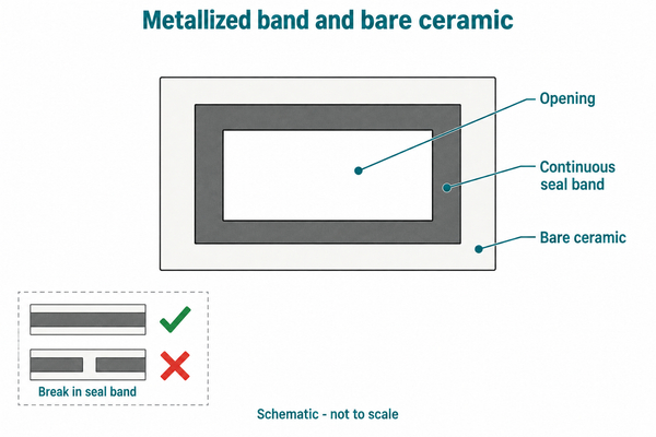
Include a sectional view when a coating wraps around an edge or continues into a bore. A top-view outline alone may not show where metal must stop. Define the permitted coating boundary, its tolerance and any required insulation distance in the assembly drawing.
Also distinguish a continuous electrical path from a continuous sealing path. A narrow break across a seal band can interrupt joining even when another part of the metallization still conducts electricity. Continuity testing cannot replace examination of the actual seal geometry.
When Should Metallization and Brazing Happen in PCB Assembly?
High-temperature metallization and package brazing generally belong before installation of heat-sensitive components. The exact sequence also depends on whether the ceramic circuit is a separate insert or part of the package body.
For a separate circuit tile, the housing can be prepared before the populated tile is installed. For an integrated ceramic structure, each subsequent heat cycle must be compatible with the existing conductors, finishes and joints. Later soldering or lid attachment must not remelt or damage an earlier connection.
Provide the planned attachment processes with the PCB drawing: die attach, wire bonding, solder assembly, housing attachment and lid sealing. Listing only the final service temperature misses the higher temperatures encountered during manufacture. A Mo-Mn firing cycle cannot be applied to an already populated ceramic PCB as a routine finishing operation.
Which Tests Check the Metallization and the Circuit?
Circuit tests and seal tests answer different questions. Electrical continuity confirms a connection; adhesion testing evaluates a bond under a specified load; leakage testing evaluates a completed enclosure. No single result substitutes for all three.
| Requirement | Suitable verification approach | What the result does not establish |
|---|---|---|
| Correct circuit connections | Netlist-based continuity and isolation checks | Seal tightness or joint strength |
| Correct metallized area | Visual and dimensional inspection against the drawing | Internal interface quality by appearance alone |
| Required coating thickness | A suitable calibrated measurement method, such as qualified XRF or cross-section measurement | Adhesion or absence of every local defect |
| Bond integrity | Specified pull, push or shear test with defined sample geometry | Hermeticity of the complete enclosure |
| Hermetic enclosure | Leak testing to an agreed method and acceptance limit | Electrical function of the PCB inside |
For a failure investigation, identify where separation occurred: ceramic, fired metallization, plated layer or braze. A failed joint does not automatically mean the PCB conductor pattern was defective. Keep substrate inspection results and package-level test records associated with the correct part and manufacturing stage.
Moly Manganese Metallization FAQs
Is molybdenum manganese alloy the same as Mo-Mn metallization?
No. "Molybdenum manganese alloy" does not fully describe the fired ceramic coating. The paste formulation and its interaction with the ceramic are essential; specifying only two metal names omits the bonding system and process conditions.
Is Mo-Mn the same as HTCC metallization?
No. HTCC co-fires a ceramic structure with compatible refractory conductors. Conventional Mo-Mn surface metallization is applied to an already fired ceramic part. Both may involve refractory metals, but their process sequences and drawing requirements differ.
Does moly manganese metallization with titanium mean active brazing?
Not necessarily. Titanium could refer to a mating component, an added material or an active constituent in a braze alloy. Titanium-containing active brazes can bond suitable ceramics by a different route from conventional Mo-Mn pre-metallization. Identify where the titanium is used before selecting the process.
Is a nickel-finished Mo-Mn coating non-magnetic?
Do not assume so. Nickel is ferromagnetic under ordinary conditions, although the magnetic behavior of a deposited coating depends on its composition and treatment. If non-magnetic ceramic metallization is required, specify that requirement before choosing the complete coating and joining system.
What Information Do We Need for a Ceramic PCB Inquiry?
Send us the circuit drawing or Gerber data, ceramic material and thickness, conductor requirements, pad finish, quantities and intended assembly processes. If the circuit interfaces with a metallized package, include the package drawing and identify the areas that require Mo-Mn separately from the circuitry.
For moly manganese metallization interfaces, include the mating metal, planned joining cycle and which party supplies and tests the completed seal. We will use these inputs to assess the ceramic circuit requirements and its assembly interfaces. Contact us at sales@bstceramicpcb.com for a ceramic PCB quotation.
 Products
 About us
 Contact us



