






















































 HOME


-

When Does a Thin-Film Circuit Need a Polished Alumina Substrate?
2026 10,18 -
Ceramic PCB for Humanoid Robot joint actuators
2026 04,07 -
LTCC PCB Surprises: What Most People Miss
2025 12,09 -
Step-by-Step Guide to DPC PCB Design for Sensor Systems
2025 12,03 -
Ceramic PCBs Essential Benefits and Applications
2025 12,01 -
How Al2O3 DPC Ceramic Substrate PCB Enhances Heat Dissipation in Modern Electronics?
2025 11,28 -
How to Choose Between Ceramic, FR4, and Metal Core PCBs
2025 11,27 -
DPC Ceramic PCB Materials: Surprising Science Inside
2025 11,26 -
Wire bondable 2-layer Alumina substrates PCB | Bstceramic PCB
2025 09,22 -
Silicon Nitride Substrate, Silicon Nitride Ceramic Substrate Formula
2025 05,08 -
What is thick film ceramic PCB?
2023 08,02
When Does a Thin-Film Circuit Need a Polished Alumina Substrate?
Published:
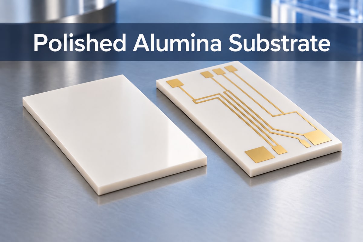
A polished alumina substrate is worth the added cost when surface texture interferes with thin-film continuity or fine circuit patterns. This article explains when polishing helps, how to choose between surface finishes, and when single-side polishing is enough—so you can avoid paying for a finish that does not improve your circuit.
At BSTCeramicPCB, our engineers help you match substrate surface requirements to your thin-film circuit design through DFM review, process compatibility advice and prototype support. A dedicated sales contact coordinates with a three-engineer technical team throughout development, helping you resolve technical questions and validate samples before moving to larger orders.
When Is a Polished Alumina Substrate Worth Using?
Choose polishing when the circuit needs a finer surface than the selected as-fired ceramic can provide. The benefit should appear in the manufactured circuit, such as more consistent film coverage or better-defined fine features.
Two situations help make the decision:
- Your existing circuit already passes on an as-fired substrate: Keep that qualified finish unless a design change creates a new requirement.
- You are introducing narrower conductors or a more demanding film stack: Evaluate a polished surface using the intended deposition and patterning process.
If the current problem comes from contamination, mounting stress or an unsuitable metal system, a smoother substrate alone may leave it unresolved. Identify the failure before adding polishing cost.
How Do As-Fired, Lapped and Polished Surfaces Differ?
Select the finish for the result you need: a usable fired surface, tighter geometry or a finer circuit face.
| Finish | Main reason to consider it |
|---|---|
| As-fired | Meets circuit needs without extra finishing |
| Lapped | Controls thickness or flatness |
| Polished | Provides a finer surface for deposited films |
Lapping and polishing can be combined. However, they are not a simple ranking from basic to best: a lapped surface is not necessarily smoother than a smooth as-fired face.
For a design needing both low roughness and tight flatness, specify both. Ordering “polished alumina” alone does not establish the finished thickness or flatness.
How Smooth Does the Surface Need to Be for Thin-Film Circuits?
Smooth enough to produce the required film and circuit features reliably. There is no universal Ra limit for every thin-film design.
The useful acceptance criteria come from the circuit:
- Continuous conductors: The deposited metal must cover the surface without unwanted breaks.
- Defined features: Patterned lines and gaps must meet the design dimensions.
- Electrical performance: The finished circuit must meet its functional requirements.
Start with the surface specification qualified for your film stack and feature sizes. If that combination is new, use representative samples to establish whether a finer finish improves the result.
When comparing quoted Ra values, use the same measurement method and conditions. Otherwise, a smaller number may not represent a meaningful improvement. Also inspect critical circuit areas: an acceptable average can conceal a damaging local defect.
Why Can a Smooth Substrate Still Cause Circuit Defects?
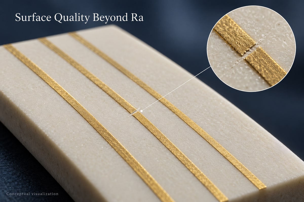
Low average roughness does not rule out local damage, contamination or poor geometry. These problems affect different parts of manufacturing:
- A scratch across a fine conductor: May disrupt the deposited path.
- A pit beneath an active film: May create a local coverage problem.
- Bow or thickness variation: Can interfere with seating and process positioning.
- Residue or particles: Can affect deposition and adhesion.
Focus inspection on where the circuit actually sits. A defect crossing a narrow conductor deserves different attention from one outside the functional area.
Protect the surface after finishing, too. Cleaning, handling and storage must preserve the condition needed for metallization; a polished surface can still arrive at deposition contaminated.
Does Higher Alumina Purity Always Mean a Better Polished Surface?
No. Higher purity does not automatically deliver lower roughness or fewer surface defects. Grain structure, porosity and the finishing process also influence the result.
Choose purity for the material properties your circuit needs. Then compare the achievable surface finish on that grade. Increasing purity solely to obtain a smoother face can add cost without addressing the actual surface problem.
For an established design, keep the qualified material unless there is a clear reason to change. For a new design, evaluate material grade and finish together on samples instead of treating the purity percentage as a surface-quality guarantee.
When Is Single-Side Polishing Enough?
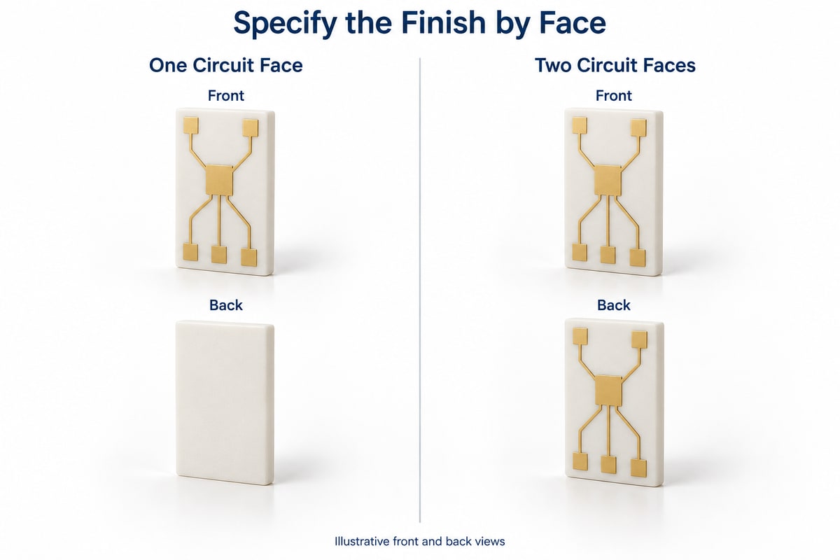
Single-side polishing is enough when only the circuit face needs the fine finish and the back already meets its mounting and processing needs.
- One functional thin-film face: Evaluate single-side polishing first.
- Fine-film features on both faces: Evaluate the required finish separately for each side.
- A back face used only for mounting: Prioritize flatness, thickness and the bonding interface; it may not need the front face’s roughness.
A backside metal layer does not automatically require double-side polishing. Its deposition process and function determine the necessary preparation.
For a ceramic bonded to a metal base, suitable low thermal expansion metals can help manage expansion mismatch. Backside polishing does not resolve that source of assembly stress.
Why Choose BSTCeramicPCB for Your Polished Alumina Substrate Project?
BSTCeramicPCB helps you evaluate the substrate finish as part of a manufacturable circuit. Our support is particularly useful when a design is moving from an initial material choice to sample validation.
- DFM review before production: R&D and PCB/PCBA engineers with 20 years of experience provide pre-review reports and process compatibility advice, helping you assess the relationship between substrate requirements and circuit fabrication.
- Prototype and small-batch support: Evaluate film quality, circuit features and assembly fit before committing to a larger run.
- Coordinated technical communication: One sales specialist and three engineers support the project, helping turn design questions into clear manufacturing requirements.
- Support through assembly: When the project includes an assembled board, PCB manufacturing, component sourcing, PCBA assembly and testing can be coordinated through one team.
Discuss your intended film process, critical features and mounting arrangement with us at sales@bstceramicpcb.com. We can help review the requirements and plan a suitable sample build.
FAQs about polished alumina substrate
Is a polished alumina substrate supplied with circuitry?
A polished blank does not automatically include circuitry. Specify whether you need a bare substrate, metallization, a patterned circuit or a complete assembly.
Does polishing improve alumina’s thermal conductivity?
It does not increase the material’s bulk thermal conductivity. Any improvement in an assembled thermal path depends on contact geometry, the interface material and the mounting arrangement.
Is polishing necessary for thick-film printing?
Not necessarily. A qualified as-fired surface may already suit the paste and firing process. Use polishing only when the printing process benefits from it and the combination has been validated.
Does lower Ra guarantee stronger metal adhesion?
No. Adhesion also depends on cleanliness, surface preparation, the metal system and deposition conditions. Evaluate adhesion using the intended process.
Can polishing meet both very low roughness and tight dimensional tolerances?
The achievable combination depends on the alumina grade, substrate size, thickness and finishing route. Review these requirements together rather than selecting each limit independently.
Move Your Ceramic Circuit Design Toward Production
Choosing BSTCeramicPCB gives you engineering support at the stages where substrate decisions affect manufacturing. Our DFM pre-review helps identify process compatibility concerns before fabrication, and prototype and small-batch support lets you evaluate the selected surface finish in your actual circuit before scaling up. For projects requiring assembly, we also coordinate component sourcing, PCBA assembly and testing, reducing the supplier handoffs you need to manage.
Send your drawings, intended application and any surface requirements to sales@bstceramicpcb.com. Whether you are developing a new polished alumina substrate design or addressing problems in an existing ceramic circuit, our engineers can help review your requirements and plan the next sample build.
 Products
 About us
 Contact us



