






















































 HOME
HOME


-

Ceramic PCB for Humanoid Robot joint actuators
2026 04,07 -
LTCC PCB Surprises: What Most People Miss
2025 12,09 -
Step-by-Step Guide to DPC PCB Design for Sensor Systems
2025 12,03 -
Ceramic PCBs Essential Benefits and Applications
2025 12,01 -
How Al2O3 DPC Ceramic Substrate PCB Enhances Heat Dissipation in Modern Electronics?
2025 11,28 -
How to Choose Between Ceramic, FR4, and Metal Core PCBs
2025 11,27 -
DPC Ceramic PCB Materials: Surprising Science Inside
2025 11,26 -
Wire bondable 2-layer Alumina substrates PCB | Bstceramic PCB
2025 09,22 -
Silicon Nitride Substrate, Silicon Nitride Ceramic Substrate Formula
2025 05,08 -
What is thick film ceramic PCB?
2023 08,02
Scribing Meaning in Ceramic PCB: Laser Scribing, Breakout and Design Notes
Published:
Scribing meaning in ceramic PCB manufacturing refers to making a controlled shallow groove, perforated line or weakened path on a ceramic substrate panel so that individual ceramic circuits can be separated later. In laser scribing, the laser does not normally cut fully through the ceramic. It prepares a clean break line while keeping the panel strong enough for printing, metallization, inspection or assembly handling.
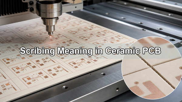
This distinction matters because ceramic materials such as alumina and aluminum nitride are hard and brittle compared with FR4. A scribe line can simplify singulation, but it must be planned together with ceramic thickness, unit size, copper layout, corner geometry, edge quality requirements and how the finished panel will be broken out.
What Does Scribing Mean in Ceramic PCB Manufacturing?
Scribing means creating a deliberate weak line in the ceramic substrate so the part can be separated from the manufacturing panel in a controlled direction. It is commonly used when multiple ceramic PCB units are produced on one larger sheet and delivered as a panel or separated after downstream processing.
In a ceramic PCB context, scribing is not just a dictionary word. It describes a manufacturing step that affects panelization, edge quality, final dimensions, handling strength and customer breakout method. A drawing that only says "cut" may not give enough information; the supplier must know whether the edge should be fully cut, partially scribed or diced.
How Does Laser Scribing Work on Ceramic Substrates?
Laser scribing works by using a focused laser to form a shallow groove or a row of closely spaced blind marks along the intended separation line. The depth is controlled so the panel remains connected during processing but can later be broken along the scribed path.
For ceramic substrates, this method is useful because the laser can create precise straight weak lines without applying mechanical force during the scribing step. The process can be used before or after certain metallization steps, depending on the stack, copper pattern, surface finish, cleanliness requirement and final panel delivery plan.
Scribing vs Laser Cutting vs Dicing: What Is the Difference?
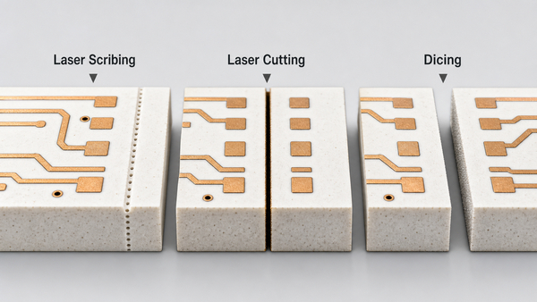
The practical difference is how much material is removed and how the part is separated. Scribing prepares a break line, laser cutting separates the part by cutting through the ceramic, and dicing uses a mechanical blade to cut along a straight path.
| Method | How It Separates the Ceramic | Best Fit | Key Risk |
|---|---|---|---|
| Laser scribing | Creates a shallow weak line for later breakout | Straight panel lines and cost-sensitive singulation | Breakout damage if thickness, size or handling method is unsuitable |
| Laser cutting | Cuts through the ceramic along the profile | Curves, internal corners, slots, holes and complex outlines | Heat-affected edge or cost increase if overused |
| Dicing | Uses a blade to mechanically cut straight lines | Wafer-like substrates or designs requiring sawed straight edges | Chipping, blade wear and kerf allowance |
For a buyer, the decision should be made from the final edge requirement backward. If the design needs internal openings, curves or tight edge tolerance, scribing alone may not be enough.
When Should Ceramic PCB Designs Use Scribing?
Ceramic PCB designs should use scribing when the part outline contains straight separation lines and the customer wants efficient panel production with controlled breakout. It is especially useful when the units can remain in a panel during printing, plating, inspection or assembly preparation.
Scribing is often suitable for rectangular or square ceramic substrates, repeated small units, thick film ceramic PCB panels and simple straight-line singulation. It is less suitable for curved edges, internal slots, small radius corners, precision holes or shapes where the break force could pass through a fragile metallized area.
How Should Scribe Lines Be Shown on a Drawing?
Scribe lines should be shown as a separate mechanical, fabrication or panelization layer so the supplier can distinguish them from full-cut edges, routed slots and copper features. The drawing should also state whether the panel will be delivered intact, partially separated or fully singulated.
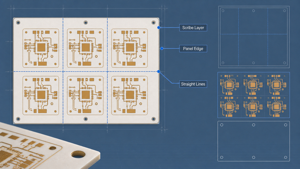
A clear drawing usually includes the panel outline, unit outline, scribe lines, full-cut lines, tooling holes, fiducials, break direction and edge tolerance. Straight scribe lines should normally extend to the panel edge or to a defined breakout boundary. If some edges need laser cutting while others need scribing, mark them with different line types or layers.
What Limits Should Be Checked Before Choosing Scribing?
The main limits are ceramic thickness, unit size, line length, copper distance from the edge, corner shape and how much force the panel can tolerate during breakout. A thicker ceramic substrate or a very small unit may require shorter scribe segments, a stronger jig or a different separation method.
- Use straight scribing lines for simple panel separation.
- Use laser cutting or machining for internal holes, slots, curves and inward corners.
- Keep copper, metallization and vias away from the scribe path according to the supplier's process allowance.
- Check whether the ceramic is alumina, AlN, BeO, ZTA or another brittle substrate material.
- Confirm whether the customer or supplier will break out the panel.
- Validate edge quality early if the substrate will be used in high-voltage, optical, sensor or sealing applications.
These checks prevent a common problem: a panel that looks economical in fabrication but becomes risky during assembly or final separation.
How Are Scribed Ceramic Panels Broken Out?
Scribed ceramic panels are usually separated by applying controlled bending force along the scribed line. Thin and simple panels may be broken by hand with proper handling, while thicker or smaller ceramic units often need a flat jig to support the panel and distribute force evenly.
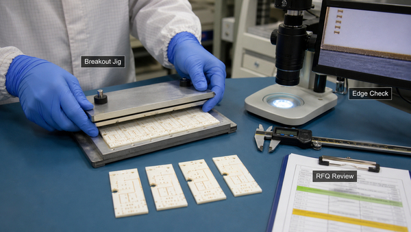
The breakout direction matters. The operator should support both sides of the scribe line, avoid twisting, keep the panel clean and prevent local stress near copper traces or finished components. If the substrate has already been assembled, breakout risk becomes higher and should be reviewed before the production route is approved.
What Edge Quality and Reliability Risks Should Be Reviewed?
Edge quality should be reviewed because ceramic edge chips, cracks or roughness can affect assembly fit, insulation distance, sealing surfaces and long-term reliability. A scribed edge is not the same as a polished cut edge, so the acceptable edge condition must be matched to the application.
For power electronics, high-voltage circuits and thermal modules, review copper-to-edge clearance, creepage requirement, plating edge exposure, cleaning residue and whether the break line passes near high-stress areas. If the part needs a very clean contour or tight outline tolerance, laser cutting or dicing may be a better route than breakout from scribing.
What RFQ Information Should You Send for Laser Scribing?
For a laser scribing quotation, send the full ceramic substrate drawing instead of only asking for scribing meaning. The supplier needs enough detail to decide whether scribing is safe, economical and compatible with the rest of the ceramic PCB process.
- Gerber, DXF, DWG or PDF drawing with separate scribe and cut layers
- Ceramic material, thickness and finished unit size
- Panel size, array layout and expected delivery form
- Copper layout, via locations and minimum copper-to-edge clearance
- Required edge quality, tolerance and inspection standard
- Whether the panel is broken out before or after metallization, assembly or testing
- Prototype quantity, mass production volume and packaging requirements
BSTCeramicPCB can review ceramic PCB drawings, panel layouts and process constraints for ceramic PCB, thick film ceramic PCB manufacturing, DPC ceramic substrates and laser-related ceramic circuit applications. For a project review, contact BSTCeramicPCB with drawings and expected production volume.
FAQ About Scribing Meaning in Ceramic PCB?
1. What is the simple meaning of scribing?
Scribing means marking or forming a controlled line on a material. In ceramic PCB manufacturing, it usually means creating a weak separation line so individual ceramic substrates can be broken out from a panel.
2. Is laser scribing the same as laser cutting?
No. Laser scribing usually does not cut fully through the ceramic. Laser cutting separates the material by cutting through the full thickness.
3. Can all ceramic PCB outlines use scribing?
No. Scribing works best for straight separation lines. Curves, inner corners, holes and slots usually require laser cutting, machining or another full-depth process.
4. Does scribing change the finished substrate size?
The final size depends on the panel design and breakout method. The scribe line must be planned with the supplier so the finished dimensions and edge tolerance are realistic.
5. What files are needed to quote ceramic PCB scribing?
Send Gerber or CAD files, material and thickness, panel drawing, scribe layer, cut layer, copper clearance, edge tolerance and whether the panel should be delivered intact or singulated.
Conclusion
Scribing meaning in ceramic PCB is best understood as controlled weak-line preparation for panel singulation. It can reduce separation cost and simplify handling when the design uses straight lines, suitable thickness and clear drawing instructions. It should not be treated as a universal replacement for laser cutting, dicing or machining.
If your ceramic substrate design needs laser scribing, panel breakout or a review of ceramic PCB manufacturing options, send your drawing, material, thickness and production quantity to sales@bstceramicpcb.com. BSTCeramicPCB can help confirm whether scribing, cutting or another singulation method is the practical route for your project.
 Products
 About us
 Contact us



