






















































 HOME


-

Ceramic PCB for Humanoid Robot joint actuators
2026 04,07 -
LTCC PCB Surprises: What Most People Miss
2025 12,09 -
Step-by-Step Guide to DPC PCB Design for Sensor Systems
2025 12,03 -
Ceramic PCBs Essential Benefits and Applications
2025 12,01 -
How Al2O3 DPC Ceramic Substrate PCB Enhances Heat Dissipation in Modern Electronics?
2025 11,28 -
How to Choose Between Ceramic, FR4, and Metal Core PCBs
2025 11,27 -
DPC Ceramic PCB Materials: Surprising Science Inside
2025 11,26 -
Wire bondable 2-layer Alumina substrates PCB | Bstceramic PCB
2025 09,22 -
Silicon Nitride Substrate, Silicon Nitride Ceramic Substrate Formula
2025 05,08 -
What is thick film ceramic PCB?
2023 08,02
Why Use a Si3N4 AMB Substrate for Automotive Inverter Reliability?
Published:
A Si3N4 AMB substrate for automotive inverter power modules combines a tough silicon nitride ceramic, thick copper and active-metal-brazed interfaces. Its purpose is to provide mechanical damage tolerance in a stack that repeatedly heats and cools. The decision is justified only when the material, copper geometry, module constraint and reliability tests address the failure mechanisms expected in the actual inverter.

What Is Specific About the Si3N4 AMB Construction?
Si3N4 is the ceramic core; AMB is the process that joins copper to it through an active-braze system. The ceramic provides electrical isolation and heat transfer, while its mechanical behavior helps the bonded stack tolerate local strain. The copper carries power and provides assembly surfaces.
This is not the same as a generic AMB process article. Here the engineering question is how silicon nitride changes crack resistance, stress distribution and validation for an automotive inverter.
Which Material Properties Matter to the Reliability Argument?
Representative published ceramic-substrate data illustrate the trade-off, but the values below are not BSTCeramicPCB purchase specifications or guarantees.
| Ceramic | Representative thermal conductivity at 20°C | Representative CTE at 20–300°C | Main reason to consider it |
|---|---|---|---|
| Al2O3 | About 24 W/m·K | About 6.8 ppm/K | Cost-effective DBC when thermal and cycling targets are met |
| Si3N4 | About 90 W/m·K | About 2.5 ppm/K | Combination of useful heat transfer and high fracture toughness |
| AlN | About 170 W/m·K | About 4.7 ppm/K | Higher ceramic heat transfer when it materially limits the stack |
Confirm the actual grade, test method and supplier data before design release. Thermal conductivity alone does not rank cycling life; strength distribution, flaw population, thickness and package constraint also matter.
How Does Thermal Expansion Load the Copper Edges?
Copper expands more than the ceramic during heating. At a copper edge or corner, that mismatch creates a local peel and shear field in the ceramic and braze region. Cooling reverses the load. Repetition can grow a pre-existing flaw even when the bulk ceramic temperature remains below a material limit.
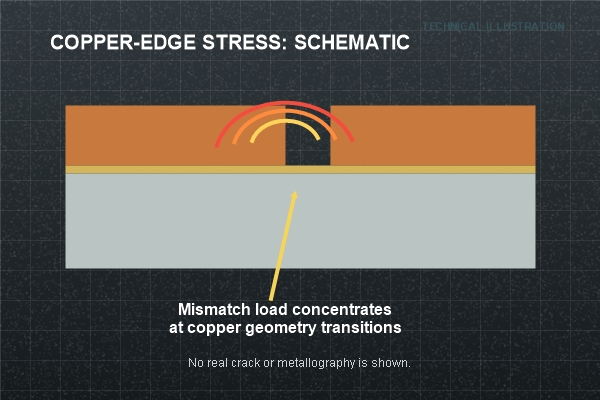
The important location is often the geometric transition, not the center of the copper island. Simulation and sectioning plans should therefore target edge radii, neck-downs, notches and areas near module constraints.
Where Can Cracks Initiate, and What Does the Path Reveal?
A ceramic crack starting below a copper corner points to a different mechanism than braze separation or a crack driven from handling damage at the substrate edge. The observed path should be mapped to geometry, thermal history and process records before corrective action is chosen.
| Observed origin or path | Likely questions to investigate |
|---|---|
| Below a copper corner | Corner radius, copper thickness, local mismatch and cycle range |
| Along the braze interface | Wetting, reaction layer, voiding, contamination and local stress |
| From the ceramic outer edge | Singulation, handling, packaging and mounting constraint |
| Near an attach void or baseplate feature | Assembly bond line, cooler flatness and local restraint |
No single image proves the root cause. Electrical symptoms, acoustic or X-ray observations, cross-sections and process history must agree.
How Can the Active-Braze Interface Fail?
The active braze must create a continuous, controlled bond between copper and Si3N4. Incomplete wetting, local discontinuity, contamination or an abnormal reaction region can reduce effective bonded area and redirect stress. Excess flow can also interfere with edge geometry or inspection.
Our Si3N4-compatible AMB ceramic substrate route for IGBT power modules is the relevant product path. We review ceramic, copper, braze construction, artwork and agreed interface evidence as one stack rather than treating the braze as an invisible adhesive layer.
How Do Copper Thickness and Pattern Shape Change the Crack Risk?
Thicker copper improves current capacity and heat spreading, but it also transfers more mechanical load into the ceramic and braze. Large copper islands, unbalanced top and bottom coverage, sharp corners and abrupt width changes can increase local strain.
The design response is not simply “use thinner copper.” Current density, thermal spreading and stress must be optimized together. Finished copper thickness, corner geometry and bottom-copper function should be stated explicitly in the drawing.
How Does the Module Constraint Change the Failure Mechanism?
The same Si3N4 AMB substrate can experience different stress when soldered to a baseplate, sintered to a cooler, clamped, or used in a baseplate-free module. Attach-layer stiffness, voiding, cooler flatness and mounting pressure change how the substrate bends and where strain concentrates.
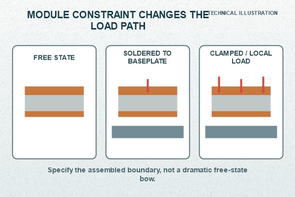
Specify the functional contact area and lower-interface process. A dramatic free-state bow image is not a useful model of real module behavior; measured flatness and assembled constraint must be evaluated under defined conditions.
What Evidence Should a Failure Analysis Preserve?
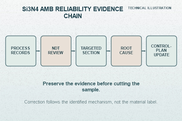
Preserve part identity, drawing revision, lot, load history, temperature history and the first electrical or thermal symptom. Record non-destructive observations before cutting. Section through the predicted origin, document the crack path and compare it with copper geometry, braze condition and assembly constraint.
The corrective action should follow the evidence. It may involve corner geometry, copper balance, braze control, edge handling, attach voiding or cooler constraint. Changing the ceramic grade without locating the origin can leave the real mechanism untouched.
Which Test Ladder Is Appropriate for Automotive Reliability?
Use increasing levels of integration so that each test answers a specific question.
| Test level | What it can establish | Main limitation |
|---|---|---|
| Material or interface coupon | Relative ceramic and braze behavior | Does not reproduce the full layout or constraint |
| Patterned substrate cycling | Geometry and bonded-stack response | Excludes die attach and cooler interaction |
| Assembled-module thermal cycling | Interaction among attach, substrate and baseplate | May not reproduce current-driven heating |
| Power cycling | Die, interconnect and substrate response under electrical load | Needs failure analysis to separate causes |
| Inverter or vehicle validation | Operation in the intended environment | Does not identify the internal root cause by itself |
Define temperature limits, dwell, ramp, sample count and failure criteria at every level. Passing a bare-substrate test does not guarantee a vehicle lifetime target.
Which Manufacturing Controls Belong to Us?
We control the released ceramic circuit scope: approved artwork, material and thickness callouts, AMB process controls, finished copper geometry, surface finish, critical dimensions, agreed electrical tests, visual criteria and traceability. We can provide prototype and production support after those requirements are frozen.
We do not convert our substrate inspection into a claim that the finished inverter is qualified. That boundary makes the evidence stronger: the customer can see which result comes from our manufacturing process and which requires module-level validation.
When Does Si3N4 AMB Earn Its Place over DBC?
Si3N4 AMB earns its place when the reliability model and tests show that toughness, active-braze construction and cycling margin solve a defined failure risk. DBC remains appropriate when it meets thermal, insulation and life targets with a simpler or lower-cost construction.
Our automotive DBC ceramic circuit and DBC ceramic substrate for IGBT semiconductors provide relevant comparison routes. The decision should be reopened only when the stack, geometry or duty-cycle evidence changes.
What Reliability and Manufacturing Package Should You Send?
For our Si3N4 AMB manufacturability review, send Gerber or ODB++ data, a dimensioned drawing, Si3N4 grade or required properties, finished ceramic and copper thicknesses, active-braze requirements when controlled, surface finish, die map, die-attach and interconnect methods, lower-interface constraint, critical analysis locations, isolation test, cycling profile, sample quantity and forecast volume.
Email the package to sales@bstceramicpcb.com. We will review the manufacturable stack and identify missing evidence before quotation. A Si3N4 AMB substrate for automotive inverter is justified when its specific material and interface behavior close a defined automotive reliability risk.
 Products
 About us
 Contact us



