






















































 HOME


-

How to Choose a LED Lighting Ceramic Printed Circuit Boards Supplier?
2026 10,16 -
Ceramic PCB for Humanoid Robot joint actuators
2026 04,07 -
LTCC PCB Surprises: What Most People Miss
2025 12,09 -
Step-by-Step Guide to DPC PCB Design for Sensor Systems
2025 12,03 -
Ceramic PCBs Essential Benefits and Applications
2025 12,01 -
How Al2O3 DPC Ceramic Substrate PCB Enhances Heat Dissipation in Modern Electronics?
2025 11,28 -
How to Choose Between Ceramic, FR4, and Metal Core PCBs
2025 11,27 -
DPC Ceramic PCB Materials: Surprising Science Inside
2025 11,26 -
Wire bondable 2-layer Alumina substrates PCB | Bstceramic PCB
2025 09,22 -
Silicon Nitride Substrate, Silicon Nitride Ceramic Substrate Formula
2025 05,08 -
What is thick film ceramic PCB?
2023 08,02
Sputtering vs Evaporation: Which PVD Process Is Better for Ceramic Thin Films?
Published:
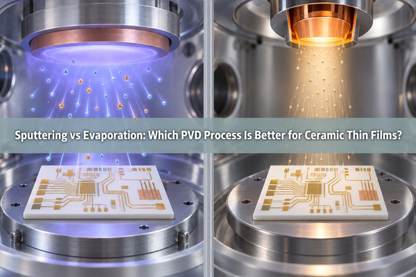
Sputtering vs evaporation compares two physical vapor deposition routes for forming metal and other thin films on ceramic substrates. Sputtering generally provides a denser film, stronger process control for alloys, and better coverage over surface features. Evaporation generally provides a more directional flux, lower particle bombardment, and an efficient route for lift-off and selected high-purity metal films. For a ceramic thin-film circuit, the correct choice also depends on the substrate finish, adhesion layer, conductor stack, patterning route, feature geometry, and acceptance tests.
How Does Sputtering Deposit Thin Films?
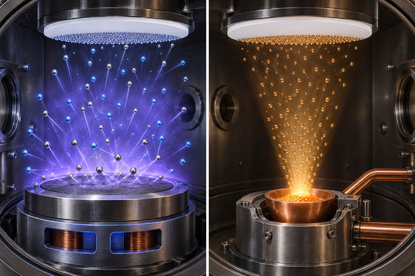
Sputtering is a PVD process in which ions from a plasma, commonly argon, strike a solid target and eject atoms from its surface. Those atoms travel through the chamber and condense on the ceramic substrate. A magnetron confines electrons near the target so that the plasma can operate efficiently, which is why magnetron sputtering is widely used for metal, alloy, adhesion, seed, and selected reactive films.
The arriving atoms have more kinetic energy than particles produced by ordinary thermal evaporation. Their trajectories are also less strictly line-of-sight because they interact with the process gas. These characteristics can support dense films, useful adhesion, and better coverage around shallow surface features. They can also increase substrate heating, bombardment, trapped gas, and residual stress if the power, pressure, bias, temperature, or deposition geometry is not controlled.
The term PVD sputtering covers several variants. DC and RF magnetron sputtering are common production methods, while ion beam sputtering is used when a different level of film control is required. Target composition, gas, base pressure, process pressure, power, and substrate preparation determine the deposited film composition and interface quality.
How Does Evaporation Deposit Thin Films?
Evaporation heats a source material until atoms or molecules enter the vapor phase and travel through a high-vacuum chamber to the substrate. Resistive thermal evaporation heats the source in a boat, filament, or crucible. E-beam evaporation directs an electron beam at the source, allowing selected higher-melting-point materials to be vaporized while the source holder remains cooled.
Because the evaporated particles travel mainly from a compact source to surfaces within line of sight, the deposited flux is highly directional. This favors lift-off: metal reaches the open resist areas while limited sidewall coating helps the unwanted film separate cleanly. The relatively low particle energy can also suit temperature- or plasma-sensitive stacks, although radiant heating and e-beam-related effects still require review.
The electron beam evaporation vs sputtering decision is not identical to comparing resistive evaporation with sputtering. E-beam broadens the material range and can provide a high deposition rate, but it remains a directional evaporation process. In e beam evaporation vs sputtering, the electron beam heats the evaporation source; it does not give the arriving vapor the same bombardment characteristics as sputtered particles.
What Is the Difference Between Sputtering and Evaporation?
| Selection factor | Sputtering | Evaporation | Why it matters on ceramic |
|---|---|---|---|
| Source mechanism | Plasma ions eject atoms from a target | Heat vaporizes or sublimes a source | Changes material compatibility and process control |
| Particle energy | Generally higher | Generally lower | Influences film density, interface formation, heating, and stress |
| Directionality | More angular scattering | Strongly line-of-sight | Affects step coverage, shadowing, and lift-off |
| Alloy and compound deposition | Target composition or reactive gas can support suitable systems | Different vapor pressures can change the deposited ratio | Important when the stack is not a single pure metal |
| Refractory materials | Often practical without melting the target | E-beam can handle selected high-melting materials; resistive sources are more limited | Constrains adhesion, barrier, resistor, or conductor choices |
| Deposition rate | Process- and material-dependent; often lower for some dielectrics | Can be high for suitable source materials | Affects cycle time, but not by itself film acceptance |
| Film coverage | Better over shallow features in many cases | Poorer on hidden or vertical surfaces | Relevant to vias, ceramic topography, and patterned resist |
| Patterning fit | Often paired with etching or seed-layer plating; lift-off needs care | Directionality is favorable for lift-off | The downstream process may decide the deposition method |
In sputtering vs thermal evaporation, fixture rotation and source-to-substrate distance affect thickness distribution, while pressure, substrate temperature, and surface preparation affect film growth and adhesion. For our ceramic circuits, we review the ceramic material, metal layers, pattern geometry, and required film thickness together when assessing the manufacturing route.
Which Process Provides Better Film Adhesion on Ceramic?
Sputtering often has an advantage because energetic arriving atoms can form a dense interface and improve nucleation. That does not mean sputtered metal automatically bonds to any ceramic. Alumina, AlN, and other ceramics are chemically stable surfaces; organic residue, moisture, polishing compound, laser residue, open pores, and weak surface particles can defeat either process.
Good adhesion starts before deposition:
- Define the ceramic grade, fired condition, and circuit-side finish.
- Clean and dry the surface with a controlled sequence.
- Use an approved activation method when the stack requires it.
- Select an adhesion or barrier layer compatible with the ceramic and top conductor.
- Control time between cleaning, activation, and deposition.
- Verify the finished stack with an agreed adhesion test and downstream thermal exposure.
Evaporated films can achieve good adhesion when the surface and stack are designed correctly. Conversely, high sputter energy can create stress or damage a sensitive underlayer. Adhesion results apply to the tested ceramic finish, surface preparation, layer materials, thicknesses, and thermal history. A change to any of these can require the interface to be tested again.
Which Process Provides Better Step Coverage on Ceramic?
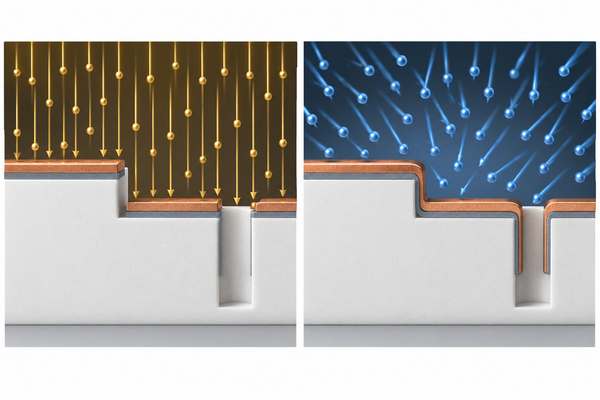
Sputtering usually covers shallow steps and non-horizontal surfaces more effectively because the deposited atoms arrive over a wider angular range. Evaporation is more directional, so raised features, recesses, steep edges, and deep holes can shadow part of the surface. Substrate rotation can improve uniformity, but it cannot make a line-of-sight process fully conformal.
This difference matters when a ceramic design contains:
- laser-drilled holes that need a continuous seed layer;
- metallization that approaches a substrate edge or shallow recess;
- ground, lapped, or polished topography with different peak heights;
- patterned resist where sidewall coating must either be minimized for lift-off or maintained for continuity;
- wraparound or edge metallization that requires a dedicated fixture and qualified angle.
Open pores and chipped edges can interrupt a thin seed layer, while contamination can weaken its bond to the ceramic. Surface preparation and repair or rejection of damaged substrates therefore precede deposition; higher particle energy alone cannot restore missing material or remove all contamination.
How Do Deposition Rate, Uniformity and Film Density Compare?
Deposition rate, uniformity, and density are separate controls. Evaporation can deposit selected materials rapidly, but thickness varies with the source geometry, angle, masking, and fixture motion. Sputtering may provide excellent wafer- or panel-level uniformity in a qualified system, yet its rate depends on target material, power, pressure, throw distance, and whether the process is reactive.
Film density is also not the same as thickness. A dense, thin adhesion layer and a thicker plated conductor serve different functions. For ceramic PCB manufacturing, we review the deposited layer as part of the full stack: adhesion or barrier layer, seed or conductor layer, plated build-up where applicable, and the final surface finish.
Layer specifications include the required thickness of each layer and its tolerance across the usable area. Sheet resistance, adhesion, and thermal or environmental requirements help us assess whether the deposited stack will meet the circuit requirements at the proposed production rate.
Which Process Is Better for Alloys and Refractory Metals?
Material behavior can decide the process before geometry does. Resistive evaporation is most convenient for source materials that can be heated cleanly without reacting with the boat or crucible. E-beam evaporation expands the range to selected high-melting-point materials. However, when alloy constituents have different vapor pressures, the deposited composition may drift from the source composition unless the process is designed around that behavior.
Sputtering can transfer suitable alloy-target compositions more directly and can deposit refractory metals without melting the target. Reactive gases can also be introduced for selected compound films. These benefits come with their own controls: target conditioning, gas purity, target erosion, arcing, particle formation, composition verification, and film stress.
The metal evaporation vs sputtering choice changes with the function of each layer. A Ti/Au stack combines an adhesion layer with a gold surface, a Cu seed layer provides a conductive base for plating, and a resistor film must achieve its specified sheet resistance. These functions set different requirements for composition, thickness, and surface condition.
How Do Heat, Plasma Exposure and Film Stress Compare?
Ceramics tolerate temperatures that would damage many polymers, but the full workpiece may also include photoresist, temporary masks, previously deposited films, brazed components, or finished surfaces. Evaporation can reduce direct ion bombardment, yet radiant heat from the source and e-beam-related effects still matter. Sputtering introduces plasma exposure and energetic particle arrival that can raise temperature and alter stress.
Residual stress can cause curling of a thin substrate, cracking at a brittle interface, line-width change after patterning, or reduced adhesion after thermal cycling. The risk depends on film material, thickness, intrinsic stress, thermal expansion mismatch, substrate thickness, deposition temperature, cooling rate, and whether both sides are balanced.
For a thin or precision ceramic, provide the flatness or bow requirement after metallization, not only before deposition. We can then review fixture support, layer balance, process temperature, panel arrangement, and the point at which flatness will be measured.
Which Patterning Methods Fit Sputtering and Evaporation?
The deposition method must fit the patterning route.
- Lift-off: Directional evaporation is often advantageous because limited sidewall coating helps the resist profile break cleanly. Sputtered films can bridge the resist sidewall, so the resist profile, film thickness, pressure, and deposition angle require tighter control.
- Subtractive etching: Sputtering can deposit a continuous blanket film that is patterned by photolithography and etching. Etchant selectivity and undercut must be reviewed for the complete stack.
- Seed layer plus electroplating: A thin deposited seed establishes electrical continuity, while electroplating builds copper thickness in selected areas. Our DPC ceramic substrate circuit board manufacturing follows this type of integrated route. The seed layer, hole coverage, photoresist, plating distribution, etching, and final finish must work as one process.
Changing the seed deposition method in a DPC flow can alter via continuity, seed adhesion, and plating current distribution. It can also change how the seed layer etches after plating, affecting line edges and residual metal between conductors.
Which Process Is Better for Thin-Film Ceramic PCBs?
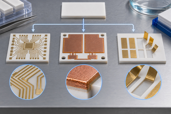
For our thin film ceramic PCB projects, we assess the deposition route against conductor geometry, layer materials, and the soldering or wire-bonding interface. Our magnetron sputtering process supports the seed and thin-film stages used with subsequent patterning and, where required, electroplating.
| Project requirement | Process normally favored | Important qualification |
|---|---|---|
| Dense adhesion or seed layer on a prepared ceramic | Magnetron sputtering | Confirm ceramic finish, cleaning, stack, stress, and adhesion test |
| Shallow topography or hole-wall continuity | Sputtering | Verify actual aspect ratio and fixture coverage; deep features may need another route |
| Directional metal deposition for lift-off | Evaporation | Confirm mask profile, shadowing, source angle, and film thickness |
| Selected pure metal at a high deposition rate | Thermal or e-beam evaporation | Confirm source compatibility, purity, uniformity, and thermal budget |
| Alloy, refractory, or reactive film | Sputtering is often favored | Confirm target composition, gas chemistry, stress, and electrical properties |
| DPC copper build-up | Sputtered seed plus electroplating | Treat deposition, plating, imaging, etching, and finish as one qualified flow |
| Plasma-sensitive or previously finished surface | Evaporation may be favored | Review radiant heat, e-beam effects, adhesion, and downstream handling |
Our thin-film circuit board design and production review also considers line width and spacing, substrate thickness, surface roughness, via or edge metallization, pad finish, wire bonding or soldering, and the required inspection records. These inputs allow us to assess the complete circuit process, including deposition, patterning, surface finishing, and the assembly interface.
How Should Sputtered and Evaporated Films Be Tested?
Film thickness, electrical resistance, adhesion, and pattern geometry establish whether the deposited layers meet the circuit requirements. Test selection depends on the metal stack, substrate, and assembly process:
| Control | What it confirms | Typical reporting form |
|---|---|---|
| Film thickness and mapping | Nominal thickness and across-part uniformity | Witness coupon, profilometry, XRF, ellipsometry, or another qualified method |
| Sheet resistance or conductor resistance | Electrical continuity and deposited/plated stack consistency | Ohms per square or defined test-pattern result |
| Adhesion | Interface performance after the agreed conditioning | Qualified tape, pull, shear, peel, or project-specific method |
| Pattern geometry | Line width, spacing, edge definition, undercut, and registration | Optical measurement and inspection images |
| Surface and defects | Particles, pinholes, scratches, discoloration, pores, and local discontinuity | Visual criteria with magnification and defect limits |
| Assembly interface | Solderability, wire bondability, die attach, or contact performance | Process-specific coupon or assembly trial |
| Environmental reliability | Stability after the actual application exposure | Thermal cycling, aging, humidity, or other agreed test |
Include the required test method, units, sample size, measurement locations, conditioning, and acceptance limits with your drawings. We use those requirements when reviewing the inspection scope for your ceramic circuit order.
Sputtering vs Evaporation FAQs
Is sputtering a form of vapor deposition?
Yes. Sputtering is one form of physical vapor deposition, alongside thermal and e-beam evaporation. In sputtering vs vapor deposition, the categories overlap: sputtering ejects atoms from a target, whereas evaporation produces vapor by heating a source. CVD uses chemical reactions to form the film.
What is the difference between PVD and CVD?
PVD transfers source material through a physical mechanism such as sputtering or evaporation. CVD forms a film through chemical reactions of gaseous precursors at or near the substrate. A PVD vs CVD decision depends on material system, temperature, conformality, chemistry, equipment, and device requirements.
Is e-beam evaporation better than sputtering?
Not universally. In sputtering vs e-beam evaporation, e-beam may be favored for directional lift-off, selected high-purity metals, and a high deposition rate. Sputtering may be favored for dense films, alloy targets, refractory materials, stronger step coverage, and a qualified ceramic seed or adhesion layer.
Is evaporation always faster than sputtering?
No. Thermal evaporation vs sputtering rates depend on source material, equipment, target or source area, power, pressure, geometry, desired thickness, and quality limits. A high instantaneous rate does not guarantee better across-part uniformity, adhesion, stress, yield, or total cycle cost.
Sputtering vs evaporation selection on a ceramic circuit depends on the layer function: a continuous seed for plated copper favors sputtering, while directional deposition through a lift-off mask often favors evaporation. Substrate finish and the required assembly interface further constrain the choice.
What Information Should a Ceramic Thin-Film RFQ Include?
For our ceramic thin-film manufacturing review, send us your drawings, stack specifications, quantity, operating environment, and acceptance requirements. Include:
- ceramic material, grade or purity, dimensions, thickness, and quantity;
- circuit-side surface condition and any roughness, flatness, bow, pore, chip, or scratch limits;
- complete metal stack, target thickness by layer, and whether each layer is deposited, plated, or finished;
- minimum line width and spacing, pad sizes, hole dimensions, edge metallization, and critical tolerances;
- preferred patterning route if it is already locked, or permission for us to propose one;
- soldering, wire bonding, die attach, contact, RF, resistor, or other functional interface requirements;
- inspection methods, coupon design, electrical tests, adhesion requirements, and reliability conditions;
- drawings, Gerber or CAD data, stack notes, prototype quantity, and production forecast.
At BSTCeramicPCB, we use your circuit drawings and layer specifications to assess manufacturability. Our production route includes magnetron sputtering and the related imaging, etching, stripping, and electroplating operations used for suitable ceramic circuits. Send the drawing and acceptance requirements to sales@bstceramicpcb.com so we can confirm the applicable process and inspection requirements.
 Products
 About us
 Contact us



