






















































 HOME
HOME


-

Ceramic PCB for Humanoid Robot joint actuators
2026 04,07 -
LTCC PCB Surprises: What Most People Miss
2025 12,09 -
Step-by-Step Guide to DPC PCB Design for Sensor Systems
2025 12,03 -
Ceramic PCBs Essential Benefits and Applications
2025 12,01 -
How Al2O3 DPC Ceramic Substrate PCB Enhances Heat Dissipation in Modern Electronics?
2025 11,28 -
How to Choose Between Ceramic, FR4, and Metal Core PCBs
2025 11,27 -
DPC Ceramic PCB Materials: Surprising Science Inside
2025 11,26 -
Wire bondable 2-layer Alumina substrates PCB | Bstceramic PCB
2025 09,22 -
Silicon Nitride Substrate, Silicon Nitride Ceramic Substrate Formula
2025 05,08 -
What is thick film ceramic PCB?
2023 08,02
Thick Film vs Thin Film Ceramic Circuits: Process, Performance and Selection
Published:
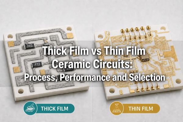
Thick Film vs Thin Film Ceramic Circuits is a process-selection question, not simply a choice between a thick metal layer and a thin one. Thick film uses printable functional pastes followed by drying and firing. Thin film uses vacuum-deposited metal, photolithography and etching or plating. That difference controls feature size, resistor behavior, surface quality, RF performance, tooling and cost. Thick film is usually the practical choice for printed resistors, heaters, rugged hybrids and cost-controlled production. Thin film is preferred when fine geometry, low noise, tight TCR, wire bonding or microwave performance justifies the more demanding process.
What Are Thick Film vs Thin Film Ceramic Circuits?
Both technologies form conductors and functional films on an electrically insulating ceramic substrate. Alumina is the most common base material, while aluminum nitride is used when the substrate must conduct substantially more heat. The ceramic is already sintered before the circuit layers are added.
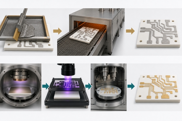
A thick film circuit is made by screen-printing conductive, resistive or dielectric paste through a patterned mesh. Each printed layer is dried and fired so that its inorganic phase bonds to the ceramic. Multiple print-and-fire cycles can create conductors, crossover dielectrics, resistors and heater patterns.
A thin film circuit starts with a very uniform metal or resistive layer deposited in a vacuum. Photoresist, exposure and etching define the pattern. Electroplating may then build selected areas to the final thickness. The term thin film describes the deposition and patterning route; a plated thin-film conductor can be thicker than the original deposited seed layer.
How Are Thick Film and Thin Film Ceramic Circuits Manufactured?
Thick film manufacturing favors repeatable printing and firing. Thin film manufacturing favors uniform deposition and precision pattern transfer.
Thick film process
- Clean and inspect the ceramic substrate.
- Screen-print conductor, resistor or dielectric paste.
- Dry the printed layer to remove the organic vehicle.
- Fire the layer with a paste-specific thermal profile, commonly near 850 C for conventional systems.
- Repeat printing and firing for additional functions.
- Laser-trim printed resistors when tighter values are required.
- Inspect adhesion, geometry and electrical performance.
Thin film process
- Polish, clean and activate the ceramic surface.
- Deposit an adhesion layer and conductor or resistor layer by sputtering or evaporation.
- Coat, expose and develop photoresist.
- Etch the unwanted film or plate selected regions from the deposited seed layer.
- Strip the resist and finish solder or wire-bond areas.
- Inspect critical dimensions, sheet resistance and surface quality.
Thick Film vs Thin Film Ceramic Circuits: Key Differences
The decision should begin with geometry and electrical function, then move to cost and production volume.
| Selection factor | Thick film ceramic circuit | Thin film ceramic circuit |
|---|---|---|
| Layer formation | Screen-printed paste and firing | Vacuum deposition plus photolithography |
| Common conductor build | Roughly 8-25 um per printed conductor layer, process dependent | Submicron deposited seed; final metal may remain thin or be plated to several microns |
| Common line/space class | About 100-150 um for robust production | About 10-25 um for precision patterns |
| Surface | More texture and rounded printed edges | Smoother film and sharper edges |
| Integrated resistors | Mature paste systems; laser trimming is common | Precise deposited resistive films with tight geometry control |
| RF behavior | Suitable when loss and geometry limits are acceptable | Better starting point for low-loss, fine-geometry microwave circuits |
| Current capability | Moderate; paste resistivity and trace geometry must be checked | Limited by thin metal unless selected areas are plated |
| Relative process cost | Lower tooling and higher print throughput | Higher vacuum, cleanroom and lithography cost |
| Best fit | Heaters, sensors, resistor networks, rugged hybrid circuits | RF modules, laser submounts, precision sensors, dense microcircuits |
These are practical ranges, not universal guarantees. Paste chemistry, substrate finish, panel size, conductor system, inspection level and supplier capability can move the limits.
How Do Line Width, Film Thickness and Surface Finish Compare?
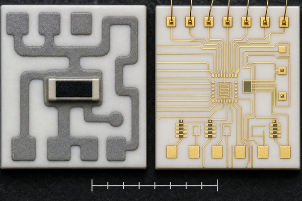
Thin film provides the tighter geometry because photolithography transfers the pattern rather than forcing paste through a mesh. It is the stronger option when narrow gaps, controlled RF structures, small wire-bond pads or dense routing drive the design.
Thick film conductors are usually wider and have a more textured surface. Screen tension, emulsion thickness, paste rheology, print speed, drying and firing shrinkage all affect the printed edge. A nominally narrow line that can be printed once is not necessarily a stable production rule across a full panel.
Film thickness alone does not determine current rating. Thick film conductors can be physically thicker than an unplated thin film, but conductive paste contains glass and other phases, so its resistivity is normally higher than pure plated copper. The useful comparison is resistance per length, temperature rise, pad structure and allowable voltage drop.
Which Technology Offers Better Precision, TCR and Noise?
Thin film is usually better for low noise, low temperature coefficient of resistance (TCR), tight matching and long-term analog stability. Vacuum-deposited resistive films such as NiCr or TaN can be formed with uniform composition and precise geometry. Typical values still depend on the specific material system and trim design.
Thick film resistors use fired composite pastes. Their resistance is affected by printed thickness, firing profile, paste lot, geometry and microstructure. Laser trimming can bring the initial value into a tight tolerance, but the engineer must also check TCR, voltage coefficient, excess noise, trim stability and pulse loading.
Use thin film when resistor matching, low-level sensor signals, calibration interval or phase/amplitude accuracy affects system performance. Use thick film when integrated resistance, environmental robustness, pulse behavior and production cost matter more than the lowest possible noise or TCR.
Which Is Better for RF, Microwave and High-Frequency Circuits?
Thin film is generally the better starting point for RF and microwave ceramic circuits. Fine lithographic edges, smooth metallization and repeatable dimensions support controlled impedance, small gaps, couplers, attenuators and compact matching networks. Gold-compatible stacks also support wire bonding and bare-die assembly.
A thin film ceramic PCB for wireless communication is relevant when the layout needs dense microstrip geometry or bondable pads. Thin film does not eliminate RF design work: insertion loss still depends on substrate dielectric data, conductor thickness, surface roughness, ground structure, launch geometry and operating frequency.
Thick film can work in lower-frequency or less geometry-sensitive RF hybrids. It becomes less attractive as line-edge definition, conductor loss and dimensional tolerance consume the RF budget. The boundary should be established with an electromagnetic model and a supplier-specific stack, not a generic frequency cutoff.
Which Is Better for Power, Current and Harsh Environments?
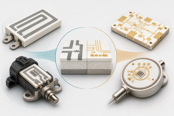
Thick film is often favored for ceramic heaters, automotive sensors, printed resistor networks and rugged hybrid modules because the printed system can integrate conductors, resistors and dielectrics in a compact structure. A thick film ceramic circuit board for scientific equipment illustrates the type of robust ceramic construction used when heat resistance and functional printing matter.
However, thick film should not be treated as a substitute for heavy copper. High-current paths may be limited by paste resistivity, terminal design and local temperature rise. When the requirement is high current or high heat flux rather than printed resistors or heaters, DPC, DBC or AMB may provide a more suitable copper structure.
Environmental reliability also depends on the complete material set. Silver-bearing thick film systems need protection where moisture, sulfur or electrochemical migration is a concern. Thin film stacks need verified adhesion, barrier layers and edge protection. In both cases, ceramic brittleness, mounting stress and thermal cycling can dominate field life.
Which Substrates and Metallization Systems Work Best?
Alumina offers the broadest process availability and is suitable for most thick film and thin film circuits. Standard 96% alumina is common in cost-sensitive thick film hybrids. Polished high-purity alumina is often used for thin film because a smooth, clean surface improves feature definition and deposited-film uniformity.
Aluminum nitride is selected when through-substrate thermal conductivity is a primary constraint. The conductor or paste system must be compatible with the AlN surface, atmosphere and assembly process. A material name alone is not enough; substrate grade, thickness, flatness, roughness and metallization stack must be defined together.
Common thick film conductors include Ag, Ag-Pd, Au, Pt-Au and controlled-atmosphere Cu systems. Common thin film stacks use an adhesion or barrier layer beneath Au, Cu or another conductor. Examples include Cr/Au, TiW/Au and Ti/Cu/Ni/Au, but the correct stack depends on soldering, brazing, wire bonding, corrosion resistance and operating temperature.
How Do Cost, Tooling and Production Volume Compare?
Thick film normally has the lower process cost when the layout can use printable geometry. Screens and firing profiles require setup, but printing supports efficient batch production and can integrate resistors or heaters without adding separate components.
Thin film uses vacuum equipment, clean processing, photomasks, lithography and more demanding inspection. That increases process cost, especially for small quantities or large substrates. The added cost is justified when fine features, stable resistors, low RF loss or wire-bond integration remove limitations elsewhere in the assembly.
Avoid fixed claims that one process is always a certain percentage cheaper. Cost changes with substrate material and size, mask count, metallization, plated thickness, tolerance, yield, trim time, inspection and quantity. The lowest-cost acceptable technology is the one that meets the real critical dimensions and electrical limits without unnecessary process capability.
When Should You Choose Thick Film or Thin Film Ceramic Circuits?
Choose the process from the requirement that is hardest to meet.
| Design condition | Practical first choice | Reason |
|---|---|---|
| Printed heater or integrated resistor network | Thick film | Functional pastes can be printed and trimmed on ceramic |
| Line/space around 100 um or larger with cost pressure | Thick film | Screen printing is productive at moderate geometry |
| Fine RF structures, small gaps or wire-bond pads | Thin film | Lithography and smooth metallization improve control |
| Low-noise, low-TCR precision resistor network | Thin film | Deposited films support tighter electrical behavior |
| Rugged hybrid sensor with moderate routing density | Thick film | Strong functional integration and mature fired systems |
| Dense medical or instrumentation microcircuit | Thin film | Fine features and stable resistive films are valuable |
| High current or very high heat flux | Compare DPC, DBC or AMB | Copper structure may matter more than film category |
| Mixed power and precision functions | Split functions or evaluate a hybrid process | One process may not optimize both zones |
A thin film ceramic circuit board for medical equipment is a useful reference for compact precision applications. The final design still needs application-specific verification rather than selection by industry name alone.
What Design and Manufacturing Constraints Matter?
The drawing must distinguish nominal values from critical acceptance limits. At minimum, review the substrate, conductor system, line/space, metal thickness, resistor geometry, pad finish, via method, edge clearance and test conditions as one process stack.
For thick film, reserve enough area for screen registration and laser-trim cuts. Avoid acute conductor corners, abrupt width changes and isolated paste features that print or fire unevenly. The number and sequence of print-and-fire cycles affect registration, surface height and cost.
For thin film, control substrate roughness, flatness and cleanliness. Define whether the metal is only a deposited film or a plated conductor build. Wire-bond pads need the correct finish, thickness and cleanliness; solder pads need a compatible barrier system.
For either process, validate adhesion, sheet resistance, isolation, critical dimensions and assembly compatibility. Thermal cycling, humidity, sulfur exposure, high-temperature storage, wire-pull or solder-shear tests should be tied to the actual failure risk rather than applied as a generic checklist.
FAQ
What is the main difference between thick film and thin film?
The main difference is how the functional layer is formed. Thick film is screen-printed from paste and fired. Thin film is deposited in vacuum and patterned by photolithography. This changes geometry, surface quality, resistor behavior, cost and applications.
What are the disadvantages of thin films?
Thin film needs vacuum deposition, clean processing and lithography, so tooling and production are more expensive. Very thin conductors also have limited current capacity unless selected regions are plated, and the process is sensitive to substrate surface quality.
What are the advantages of thick film resistors?
Thick film resistors can be printed directly into a ceramic hybrid, cover a wide resistance range and be laser-trimmed. They support productive manufacturing and can offer good pulse and environmental performance when the paste and protection system are matched to the application.
What is the typical thickness of a thick film conductor?
A common fired conductor range is about 8-25 um per printed layer, but paste type, screen, firing and the number of prints can change the result. The supplier's process capability should control the drawing value.
Is thin film always better for ceramic circuits?
No. Thin film is better when fine geometry, low noise, tight TCR or RF performance matters. Thick film is often more economical and better suited to printed heaters, resistors and rugged hybrids.
Which technology has lower electrical noise?
Thin film resistive systems generally provide lower excess noise because the deposited film is more uniform. The actual result depends on resistor material, geometry, resistance value, trim and operating voltage.
Can thick film replace thin film?
Yes, when the design can accept the thicker geometry, surface roughness, TCR, noise and tolerance of the selected thick film system. It should not replace thin film by cost alone when RF or precision limits are critical.
Can thick film and thin film be combined?
They can be combined at a module or assembly level, but combining both process families on one substrate is supplier-specific and may add handling, masking and compatibility risks. Splitting power and precision functions across separate substrates is often simpler.
Does film choice change ceramic thermal conductivity?
The substrate material and thickness dominate through-substrate thermal conductivity. Film choice changes conductor resistance, interface behavior and heat spreading, but it does not turn alumina into aluminum nitride.
Is thick film suitable for high-frequency circuits?
It can be suitable when conductor loss and geometry tolerance fit the frequency and impedance budget. Thin film is usually preferred for fine microwave structures, low loss and precise repeatability.
Conclusion
Thick Film vs Thin Film Ceramic Circuits should be decided by the most restrictive electrical and manufacturing requirement. Thick film is the efficient route for printed functions, rugged hybrids and moderate geometry. Thin film earns its higher process cost when fine features, stable resistors, low noise, wire bonding or RF performance matter. For high current or high heat flux, compare plated or bonded copper ceramic processes before forcing either film technology into the design.
BSTCeramicPCB can review the ceramic substrate, metallization stack, critical dimensions and prototype validation plan for thick film or thin film projects. For technical support, contact sales@bstceramicpcb.com.
 Products
 About us
 Contact us



