






















































 HOME
HOME

-

Ceramic PCB for Humanoid Robot joint actuators
2026 04,07 -
LTCC PCB Surprises: What Most People Miss
2025 12,09 -
Step-by-Step Guide to DPC PCB Design for Sensor Systems
2025 12,03 -
Ceramic PCBs Essential Benefits and Applications
2025 12,01 -
How Al2O3 DPC Ceramic Substrate PCB Enhances Heat Dissipation in Modern Electronics?
2025 11,28 -
How to Choose Between Ceramic, FR4, and Metal Core PCBs
2025 11,27 -
DPC Ceramic PCB Materials: Surprising Science Inside
2025 11,26 -
Wire bondable 2-layer Alumina substrates PCB | Bstceramic PCB
2025 09,22 -
Silicon Nitride Substrate, Silicon Nitride Ceramic Substrate Formula
2025 05,08 -
What is thick film ceramic PCB?
2023 08,02
When Should You Use a Thin Film Alumina Ceramic PCB?
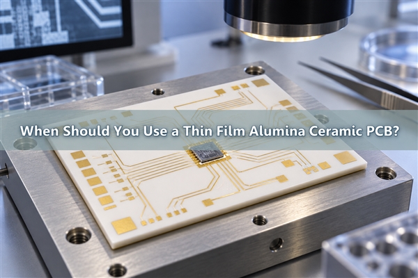
A thin film alumina ceramic PCB is the right choice when a circuit needs accurately patterned metal, a stable insulating base, and a surface suitable for wire bonding or bare-die assembly. It is commonly considered for RF, microwave, photonic, sensor, and precision hybrid circuits. It is unnecessary when ordinary thick-film printing, DPC copper, or FR4 already meets the required geometry, current, heat flow, and cost target.
What Does Thin Film Alumina Ceramic PCB Mean?
The term describes a ceramic circuit in which a thin metal system is deposited and patterned on an alumina substrate. Here, "thin film" refers to the circuit metallization, not a thin coating of alumina deposited on another material. That distinction matters because searches for alumina thin film can also lead to coatings, optical films, or materials research unrelated to PCB fabrication.
A thin film ceramic PCB differs from a conventional printed circuit board in both substrate and conductor formation. Alumina provides electrical insulation, dimensional stability, and a rigid surface. Vacuum deposition and photolithographic patterning create the conductor geometry. The combination is useful when pad definition, conductor consistency, and compatibility with chip-level interconnects matter more than high copper current capacity.
How Is Thin-Film Metallization Built on Alumina?
The process normally begins with a cleaned, flat alumina surface. An adhesion metal is deposited first because noble metals do not bond reliably to bare ceramic by themselves. A barrier or diffusion-control layer may follow, then a top conductor selected for electrical performance and the intended attachment process. Photolithography and etching define the circuit pattern.
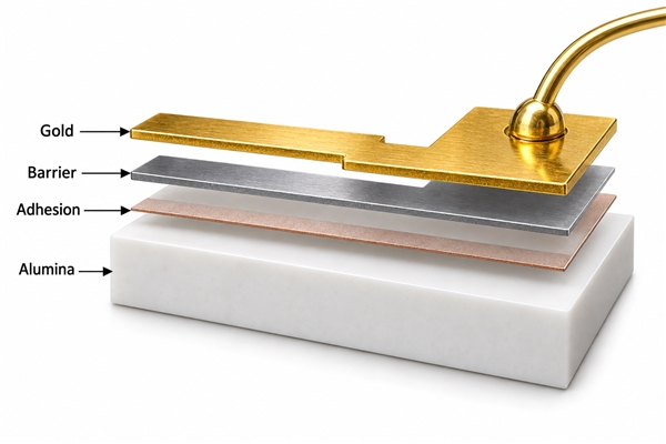
The illustration is a conceptual stack, not a universal recipe. Gold, copper, nickel, platinum, palladium, titanium, and other metals can appear in different combinations. The correct system depends on whether the finished pads will be wire bonded, soldered, brazed, die attached, or contacted by conductive adhesive. A metal stack should therefore be specified by function and final thickness, not only by the visible top-metal color.
Which Alumina Grade Is Suitable for Thin-Film Circuits?
Thin film alumina substrates are usually selected by surface condition, dielectric behavior, thermal requirement, and cost. Higher-purity alumina is often preferred for precision circuits because it can provide a smoother, more uniform surface. Standard 96% alumina may still be practical for less demanding layouts if its roughness, flatness, and defect limits are qualified for the actual pattern.
| Selection factor | Why it matters | Engineering decision |
|---|---|---|
| Alumina purity | Affects microstructure, surface quality, dielectric behavior, and cost | Use the lowest grade that still meets pattern, RF, insulation, and reliability limits |
| Surface roughness | Influences film continuity, adhesion, conductor edge definition, and RF loss | Set a measurable finish requirement instead of specifying purity alone |
| Substrate thickness | Changes stiffness, thermal resistance, impedance geometry, and handling risk | Model electrical and mechanical behavior with the finished thickness |
| Flatness and warpage | Affects lithography focus, die attach, sealing, and assembly coplanarity | Define the measurement method, panel size, and post-metallization condition |
| Edge and hole quality | Chips and microcracks can initiate fracture during assembly or cycling | Review routing, laser processing, support, and inspection criteria |
Choosing 99.6% alumina by habit can raise material and processing cost without improving the finished circuit. Conversely, choosing 96% material solely to reduce price can create yield or RF problems if the required conductor definition depends on a smoother surface.
What Performance Can Thin-Film Alumina Provide?
The main benefit is controlled circuit geometry on a stable ceramic base. Thin conductors can support precision resistive networks, compact matching structures, fine wire-bond pads, and short chip-to-circuit interconnects. Alumina also provides electrical isolation and typically conducts heat better than FR4, although it does not approach the thermal conductivity of aluminum nitride.
| Performance objective | What thin-film alumina contributes | What must still be verified |
|---|---|---|
| RF and microwave stability | Rigid dielectric geometry and accurately defined conductors | Dielectric constant, loss tangent, thickness tolerance, metal thickness, and roughness at frequency |
| Wire bonding | Fine pads and compatible noble-metal surfaces | Top-metal composition, cleanliness, bond method, wire material, and pull strength |
| Bare-die attachment | Short interconnects and stable chip placement | Attach material, planarity, metallization compatibility, voiding, and reflow or cure profile |
| Thermal transfer | An electrically insulating heat path through the ceramic | Full stack resistance, heat-spreading area, interfaces, and heatsink condition |
| Dimensional control | Low moisture uptake and stable inorganic substrate | Finished tolerance after metallization, cutting, holes, and assembly loading |
Thin Film Alumina vs Thick Film and DPC
The decision is driven by conductor geometry, metal thickness, integrated functions, attachment method, current, and production cost. These processes are not interchangeable labels for the same ceramic board.
| Process | Best fit | Main advantage | Main boundary |
|---|---|---|---|
| Thin film | RF networks, photonic submounts, precision hybrids, fine wire-bond pads | Controlled, repeatable conductor definition and chip-level interfaces | Thin metal limits current and heat spreading; process cost must be justified |
| Thick film | Printed resistors, heaters, sensors, and cost-sensitive hybrid circuits | Conductors, resistors, and dielectrics can be screen printed and fired | Coarser geometry and paste-dependent electrical properties |
| DPC | LED modules, sensors, optoelectronics, and layouts needing plated vias or thicker copper | Finer copper features than heavy bonded copper with more conductor thickness than thin film | Plating uniformity, via geometry, adhesion, and copper stress require control |
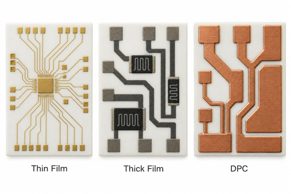
Use thin film when conductor precision or the chip interface is the deciding factor. Use thick film when printed functional materials and cost dominate. Use DPC when the design needs plated copper, vias, or more current and lateral heat spreading than a thin-film metal system can provide.
Where Is Thin-Film Alumina Used?
In RF and microwave circuits, thin-film alumina supports matching networks, attenuators, filters, couplers, and transmission-line structures. The substrate grade and finished metal geometry must be included in the electromagnetic model; using a generic alumina dielectric value can shift impedance or insertion loss.
Photonic and optoelectronic modules use fine metal traces and wire-bond pads to connect laser diodes, photodiodes, detectors, and control chips. Short interconnects and controlled placement help reduce parasitics. BSTCeramicPCB's thin film ceramic PCB for wireless communication is relevant when stable ceramic geometry and patterned metal are required for compact signal circuits.
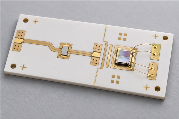
Medical sensors, analytical instruments, and precision hybrid assemblies may use alumina to isolate electrodes, interconnect bare dies, or maintain stable geometry. A thin film ceramic circuit for medical equipment illustrates this application class, but the final design still needs material, cleaning, surface finish, and reliability requirements appropriate to the device.
Automotive controls and harsh-environment sensors can also use thin-film ceramic circuits where temperature stability and compact interconnection are important. The thin film ceramic substrate for a vehicle control system is a relevant product example; system qualification must still cover vibration, temperature cycling, contamination, and mechanical support.
What Design Limits Should Engineers Review?
Published micron-scale thin-film examples from the wider industry are not a substitute for a manufacturer's released design rules. At BSTCeramicPCB, our current thin-film capability table lists conductor thickness from 5 to 13 μm, minimum trace/space of 0.15/0.20 mm, substrate thickness from 0.25 to 2.0 mm, panels up to 200 x 200 mm, and as many as 10 layers. It also lists a 0.10 mm minimum hole and ±0.10 mm hole-position tolerance. These values remain subject to review of the alumina grade, metal system, panel utilization, tolerances, and test requirements.
Mechanical design deserves the same attention as conductor geometry. Alumina is stiff but brittle. Large unsupported areas, sharp internal corners, closely spaced edge holes, point loads, and housing distortion can initiate cracks. Copper or metal balance, die-attach area, wire-bond access, edge clearance, and mounting support should be checked on the complete assembly.
What Production Inputs Must Be Defined?
A manufacturable release must define the substrate and metal system as a controlled stack, not as a generic "alumina PCB." The fabrication drawing and data package should agree on alumina purity or grade, finished substrate thickness, outline, holes, flatness, conductor materials, final metal thickness, minimum geometry, and surface-finish areas.
Assembly inputs should identify every joining method. Wire bonding requires the wire material, bond process, pad finish, pad size, and pull-test expectation. Soldering or brazing requires alloy, peak temperature, atmosphere, wettable area, and allowable voiding. Bare-die attachment requires die dimensions, attach material, placement tolerance, planarity, and thermal path. A fast-turn thin film ceramic PCB assembly should preserve these production materials and interfaces if the prototype is expected to predict series behavior.
When Is Thin-Film Alumina Unnecessary?
Thin film is unnecessary when the smallest features, pad tolerances, and electrical behavior can be achieved by thick film at lower processing complexity. DPC is usually more suitable when the board needs thicker copper, plated vias, higher current, or stronger lateral heat spreading. FR4 remains preferable for large multilayer routing, connectors, mechanical compliance, rework, and cost-sensitive electronics that do not need a ceramic substrate.
Alumina itself may also be the wrong ceramic when substrate thermal resistance dominates the junction-to-case path. In that case, aluminum nitride may reduce temperature rise, provided its higher material and processing cost is justified. The decision should come from the full thermal model rather than a conductivity comparison alone.
Thin Film Alumina Ceramic PCB FAQ
Is thin film alumina the same as an alumina thin film?
Not always. In ceramic PCB manufacturing, thin film alumina usually means a thin metal circuit patterned on an alumina substrate. In materials science, an alumina thin film can mean an aluminum-oxide coating deposited on another material.
Can a thin-film alumina board carry high current?
It can carry signal and moderate current within the allowed metal thickness and temperature rise, but it is not the first choice for high-current power paths. DPC, DBC, or AMB provides substantially thicker copper for current capacity and heat spreading.
Is 99.6% alumina always required?
No. Higher purity is often selected for smoother surfaces and demanding electrical or pattern requirements, but 96% alumina may be suitable when the qualified surface, geometry, thermal, and reliability limits are met.
Can gold wire be bonded directly to the circuit?
Only when the complete top-metal and barrier system is compatible with the selected wire-bond process. Surface cleanliness, metal thickness, pad geometry, bond parameters, and pull testing must be controlled.
Conclusion
A thin film alumina ceramic PCB is justified by precision conductor geometry, stable RF behavior, bare-die or wire-bond interfaces, and compact ceramic packaging. It should not be selected merely because "thin film" sounds more advanced. Alumina grade, surface condition, metal stack, feature limits, assembly method, and reliability testing must work as one manufacturing system.
BSTCeramicPCB can review the ceramic grade, thin-film metallization, layout, attachment method, and test requirements against our current process capability. For technical communication about an existing design, contact sales@bstceramicpcb.com.
 Products
 About us
 Contact us



