






















































 HOME
HOME


-

Ceramic PCB for Humanoid Robot joint actuators
2026 04,07 -
LTCC PCB Surprises: What Most People Miss
2025 12,09 -
Step-by-Step Guide to DPC PCB Design for Sensor Systems
2025 12,03 -
Ceramic PCBs Essential Benefits and Applications
2025 12,01 -
How Al2O3 DPC Ceramic Substrate PCB Enhances Heat Dissipation in Modern Electronics?
2025 11,28 -
How to Choose Between Ceramic, FR4, and Metal Core PCBs
2025 11,27 -
DPC Ceramic PCB Materials: Surprising Science Inside
2025 11,26 -
Wire bondable 2-layer Alumina substrates PCB | Bstceramic PCB
2025 09,22 -
Silicon Nitride Substrate, Silicon Nitride Ceramic Substrate Formula
2025 05,08 -
What is thick film ceramic PCB?
2023 08,02
Transparent Circuit Board Guide: Ceramic, Glass, PET and Clear Trace Design
Published:
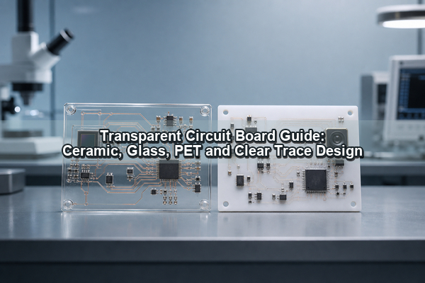
A transparent circuit board uses an optically clear or translucent substrate so light, displays, sensors, or mechanical features remain visible through selected areas of the assembly. The term can describe several very different constructions, including PET circuits, transparent polyimide flex circuits, glass-based boards, and translucent ceramic circuits. The correct choice depends on more than appearance: conductor resistance, operating temperature, heat flow, bending, drilling, component assembly, and the required optical window all affect feasibility.
What Is a Transparent Circuit Board?
A transparent circuit board is a printed or deposited electrical circuit built on a substrate that transmits visible light. It differs from a conventional FR-4 PCB because the base material is not an opaque glass-fiber epoxy laminate. Depending on the construction, the substrate may be flexible PET, transparent polyimide, glass, quartz, sapphire, or a translucent ceramic.
Transparency is usually selective rather than absolute. The substrate may transmit light, while copper traces, plated pads, solder, components, adhesives, coverlay, and solder mask remain visible. The practical design objective is therefore to preserve a defined optical path while maintaining the electrical and mechanical functions of the circuit.
Is a Transparent PCB Board Fully Transparent?
A transparent pcb board is rarely invisible after fabrication and assembly. Three separate properties determine the final appearance:
- Substrate transmission: how much light passes through the bare PET, PI, glass, quartz, sapphire, or ceramic.
- Conductor coverage: how much of the viewing area is blocked by copper, silver, metal grids, pads, planes, and vias.
- Assembly coverage: how much light is lost through components, solder joints, protective coatings, labels, connectors, and mechanical fixtures.
To keep a circuit board transparent in the required area, the optical window should be defined before routing begins. Traces can be moved around that window, narrowed where current permits, or replaced with a transparent conductor when its higher resistance is acceptable. Solid ground planes generally conflict with a large clear viewing area, so grounding may require perimeter routing, a fine conductive grid, or a separate opaque section.
Which Materials Are Used for Transparent Circuit Boards?
The substrate determines the available manufacturing process and assembly temperature. PET is economical and flexible but has a limited thermal window. Transparent polyimide tolerates higher processing temperatures and repeated flexing, although it usually has a visible tint. Glass provides strong optical clarity and dimensional stability but is brittle. Quartz and sapphire are selected when optical, temperature, dielectric, or chemical requirements justify their higher processing cost. Translucent alumina-based ceramics offer electrical insulation, dimensional stability, and better heat handling than polymer films, but they are not equivalent to optical glass.
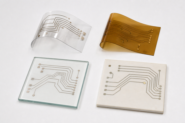
The word “transparent” should always be supported by a wavelength range, thickness, surface finish, and minimum transmission requirement. A material that appears clear in a thin sample may become hazy or only translucent at production thickness. Surface roughness, metallization, laser processing, and coatings can also change the optical result.
How Do Ceramic, Glass, PET, and Transparent PI Compare?
Material selection starts with the dominant constraint. PET suits low-temperature flexible circuits. Transparent PI is preferable when flexibility and a wider assembly window are both required. Glass provides a flat optical platform. Ceramic is more appropriate when electrical insulation, dimensional stability, local heat spreading, or harsh-environment performance matters more than glass-like clarity.
| Substrate | Optical Character | Mechanical Behavior | Thermal / Assembly Consideration | Typical Fit |
|---|---|---|---|---|
| PET | Clear film | Flexible; suitable for static bends | Low process-temperature margin | Touch panels, indicators, low-power transparent circuits |
| Transparent PI | Clear to lightly tinted | Flexible; better fatigue resistance than rigid glass | Wider thermal window than PET | Flexible sensors, compact optical assemblies, wearable electronics |
| Glass / quartz | High clarity when surfaces and coatings are controlled | Rigid and brittle; edge and hole design are critical | Dimensionally stable; assembly process must control thermal shock | Displays, optical sensors, laboratory and photonic assemblies |
| Sapphire | Optically clear over a useful wavelength range | Hard, rigid, and difficult to machine | High-temperature and chemically resistant platform | Specialized optical, RF, sensor, and harsh-environment modules |
| Translucent ceramic | Translucent rather than glass-clear | Rigid; stable but brittle | Useful electrical insulation and heat handling | LED, laser, sensor, and visible-structure ceramic circuits |
No single row is the universal “best” option. An optical sensor may favor glass or quartz, while a high-power light source may need a ceramic platform even if the result is translucent rather than fully clear.
How Are Conductive Traces Made Transparent?
Conventional copper is highly conductive but opaque. A transparent PCB can still use copper if the traces are narrow and routed outside the main optical window. This approach preserves low electrical resistance and familiar solderable pads, but the conductor pattern remains visible.
Transparent conductor options include indium tin oxide (ITO), conductive metal oxides, silver nanowires, conductive meshes, and very fine metal grids. These materials can transmit more light than solid copper, but their sheet resistance, contact resistance, adhesion, environmental stability, current capacity, and solderability must be evaluated. Transparent conductors are often suitable for sensing electrodes, touch interfaces, heaters, or low-current signal paths. They are generally less suitable than copper for power rails and high-current connections.
A hybrid layout is often more practical: transparent conductors serve the viewing or sensing zone, while copper or silver metallization is retained for component pads, connectors, current-carrying paths, and edge routing.
How Is a Transparent Circuit Board Manufactured?
The manufacturing route changes with the substrate and conductor system. A flexible PET or PI circuit may use laminated copper followed by imaging and etching, or printed conductive ink followed by curing. Coverlay or protective coating is then applied only where it does not compromise the required optical area.
Glass, quartz, sapphire, and ceramic substrates usually need deposition, printing, plating, or fired metallization processes rather than standard FR-4 lamination. Surface preparation is especially important because conductor adhesion depends on cleanliness, roughness, activation, and the compatibility of the metal system with the substrate. Holes and profiles may require laser processing, mechanical machining, scribing, or specialized cutting.
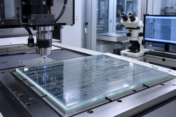
Registration also affects visual quality. Misalignment between front and back conductors can make a double-sided design appear denser than intended. For a large transparent circuit board, flatness, handling fixtures, edge quality, and panel support become increasingly important because glass and ceramic cannot absorb mechanical stress like a thin polymer film.
How Do Copper Coverage, Layers, and Solder Mask Affect Transparency?
Optical transmission should be treated as an area budget. Begin with the bare substrate, then subtract the area and losses caused by conductors, pads, vias, mask, adhesive, coverlay, components, and mounting hardware. A nominally clear substrate can still produce a visually opaque assembly when copper density is high.
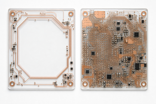
- Keep solid planes outside the primary viewing area when electrical performance allows.
- Align conductors on opposite sides where overlap can reduce the apparent blocked area.
- Use local solder mask or coverlay openings instead of coating the full optical window.
- Place test pads, fiducials, connectors, and labels in an opaque border or service zone.
- Check whether a mesh ground or perimeter return path provides adequate EMC performance.
Additional layers improve routing freedom but reduce transparency through more conductors, dielectric interfaces, adhesives, and registration tolerances. Multilayer transparent circuits are possible in selected technologies, but a two-layer or hybrid construction often preserves optical performance more effectively.
What Electrical and Thermal Limits Matter?
Transparent materials do not remove the need for current, voltage, dielectric, and temperature calculations. Narrow copper traces increase resistance and temperature rise. Transparent conductors have much higher sheet resistance than bulk copper, so trace length and current must be controlled. High-voltage designs still require creepage and clearance distances based on the operating environment and applicable standard.
Thermal behavior varies widely. PET is unsuitable for the temperatures used by many conventional soldering processes. Glass can tolerate temperature but remains vulnerable to thermal shock and local stress. Transparent PI provides a wider assembly window than PET but does not spread heat like ceramic. A ceramic circuit can conduct heat away from a local LED, laser, or sensor region while maintaining electrical isolation, although optical transmission depends strongly on ceramic composition, thickness, porosity, and surface finish.
For heat-generating devices, calculate the complete thermal path from junction through pad, conductor, substrate, interface material, and heat sink. Substrate transparency alone is not a thermal specification.
Can a Transparent Circuit Board Support SMT and Vias?
Yes, but the compatible process depends on the substrate. Transparent PI can support SMT when the adhesive, copper, coverlay, and component process are designed for the intended reflow profile. PET circuits commonly need low-temperature solder, conductive adhesive, crimped contacts, or other attachment methods. Glass and ceramic can accept metallized pads and mounted components, but pad adhesion, local stress, CTE mismatch, solder volume, and heating rate require control.
Vias are also technology-dependent. Flexible circuits may use plated through-holes or laser microvias. Glass, quartz, sapphire, and ceramic may use laser-drilled, mechanically drilled, filled, or metallized holes where the material and thickness permit. Every via placed in an optical window creates a visible feature, so routing and interconnection should be planned around the required field of view.
Where Are Transparent Circuit Boards Used?
Transparent circuits are most useful when electronics must share space with light, a display, a sensor, or a visible mechanical structure. Common application categories include:
- optical sensors and detector windows;
- LED and laser modules with visible light paths;
- transparent heaters, touch electrodes, and capacitive interfaces;
- display overlays and illuminated control panels;
- wearable and flexible electronics;
- laboratory, photonic, and educational assemblies where the circuit must remain visible;
- architectural, automotive, and consumer interfaces with integrated lighting.
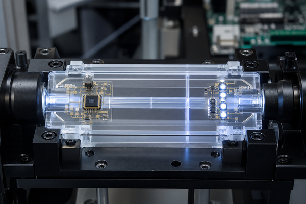
For optical and lighting designs, related ceramic platforms include laser equipment DPC ceramic circuit boards and alumina DPC ceramic substrates for LED assemblies. Sensor layouts may also benefit from the fine-feature approach used in Al2O3 DPC ceramic substrate designs for sensors.
How Should a Transparent Circuit Board Material Be Selected?
Start with the optical requirement: wavelength, minimum transmission, haze, viewing angle, clear-area dimensions, and whether the conductors may remain visible. Then establish the electrical load, including maximum current, voltage, acceptable resistance, signal frequency, grounding, and shielding. These values determine whether a transparent conductor is practical or whether copper must be retained.
Next, match the mechanical and assembly conditions. Flexible products need a defined bend radius and cycle requirement. Glass and ceramic designs need controlled edges, hole positions, mounting loads, and support. The component attachment method must fit the material's temperature window and conductor system. Finally, verify environmental conditions such as humidity, chemical exposure, UV, thermal cycling, and cleaning.
Where heat flow and electrical isolation dominate, a ceramic route may be more appropriate than a fully clear polymer or glass board. The thermal design principles used for a DPC Al2O3 ceramic substrate can be reviewed alongside the optical requirements before the stack-up is fixed.
FAQ About Transparent Circuit Boards
Can you make a clear PCB?
Yes. PET, transparent PI, glass, quartz, sapphire, and selected translucent ceramics can all support circuit patterns. The achievable clarity depends on substrate thickness, conductor coverage, surface finish, coatings, layer count, and assembly. A clear substrate does not make copper traces or components transparent.
Can transparent traces carry high current?
Transparent conductors are normally more resistive than copper and are best suited to low-current electrodes, sensors, heaters, and signal paths. High-current paths usually require wider conductors, fine metal grids, parallel paths, or a hybrid layout with copper outside the optical window.
Can a transparent PCB be multilayer?
Selected flexible, glass, and deposited-film technologies can form multiple conductive layers. However, every additional conductor and adhesive interface reduces optical clarity and increases registration complexity. A simpler layer count is preferable when a large clear area is the priority.
Is a glass PCB the same as a transparent ceramic PCB?
No. Glass is generally chosen for optical clarity and dimensional stability. Transparent or translucent ceramic is selected when electrical insulation, temperature capability, mechanical stability, or heat handling is more important. Their machining, metallization, failure modes, and achievable transmission are different.
Can transparent boards use ordinary solder mask?
They can use compatible mask or coverlay, but a conventional full-area coating may reduce transmission or add color and haze. Local protection around pads and conductors is often more suitable than covering the entire optical window.
Conclusion
A successful transparent circuit board begins with a defined optical window and a realistic conductor strategy. PET and transparent PI support flexible formats; glass, quartz, and sapphire provide rigid optical platforms; translucent ceramic is useful when heat, insulation, and dimensional stability outweigh glass-like clarity. The layer count, copper coverage, coating, via pattern, component attachment, and thermal path should be evaluated together.
BSTCeramicPCB can review ceramic substrate, metallization, layout, and assembly requirements for optical, LED, laser, and sensor applications. For a feasibility discussion, contact sales@bstceramicpcb.com.
 Products
 About us
 Contact us



