






















































 HOME
HOME

-

Ceramic PCB for Humanoid Robot joint actuators
2026 04,07 -
LTCC PCB Surprises: What Most People Miss
2025 12,09 -
Step-by-Step Guide to DPC PCB Design for Sensor Systems
2025 12,03 -
Ceramic PCBs Essential Benefits and Applications
2025 12,01 -
How Al2O3 DPC Ceramic Substrate PCB Enhances Heat Dissipation in Modern Electronics?
2025 11,28 -
How to Choose Between Ceramic, FR4, and Metal Core PCBs
2025 11,27 -
DPC Ceramic PCB Materials: Surprising Science Inside
2025 11,26 -
Wire bondable 2-layer Alumina substrates PCB | Bstceramic PCB
2025 09,22 -
Silicon Nitride Substrate, Silicon Nitride Ceramic Substrate Formula
2025 05,08 -
What is thick film ceramic PCB?
2023 08,02
Wire Bondable Ceramic Substrates: Surface Finishes and Design Guide
A wire bondable ceramic substrate has metal pads that can form repeatable wire bonds without non-stick defects, pad lift, excessive intermetallic growth, or damage to the ceramic circuit. Bondability is not guaranteed by the word “gold” alone. It depends on the complete metallization stack, surface condition, wire material, bonding method, pad geometry, cleaning history, and qualification limits.
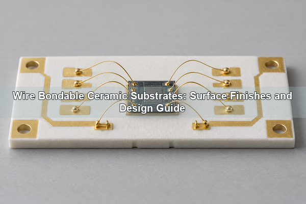
What Does Wire Bondable Mean?
Wire bondable describes a pad surface that is compatible with a defined wire-bond process. The bond must meet the required electrical resistance, mechanical strength, failure mode, and reliability after the assembly’s thermal and environmental exposures. A finish can be solderable yet unsuitable for wire bonding, and a surface that bonds during a prototype trial may still be unstable in volume production.
The specification must therefore name the wire material and diameter, ball or wedge process, pad metallization, final finish, test method, and acceptance criteria. Without those inputs, “wire bondable” is only an intention, not a measurable manufacturing requirement.
Why Do Ceramic Substrates Need a Qualified Bonding Surface?
Alumina, aluminum nitride, and silicon nitride provide electrical insulation and dimensional stability, but the ceramic itself is not the bond pad. The wire attaches to a deposited, printed, plated, or co-fired metal system. Adhesion between that metal system and the ceramic must survive ultrasonic energy, local deformation, pull force, temperature cycling, and package stresses.
Ceramic circuits are also less forgiving of localized mechanical damage than organic laminates. Excessive bond force can crack a thin ceramic, deform a soft pad, or detach a poorly adhered conductor. The substrate thickness, support fixture, pad position, and metallization adhesion should be evaluated as one assembly system.
Which Metallization Stacks Are Wire Bondable?
Select the stack from the wire material, bond method, operating environment, and manufacturing route. The entries below are common starting points, not universal approval limits.
| Metallization or finish | Typical bond use | Main advantage | Engineering caution |
|---|---|---|---|
| Fired thick-film gold | Gold or aluminum wire on qualified hybrid circuits | Direct gold surface on alumina; established for thick-film hybrids | Paste chemistry, firing profile, porosity, glass content, and surface condition affect bondability |
| Electroplated soft gold over nickel | Gold wire and selected wedge-bond processes | Controlled noble-metal surface with a diffusion barrier | Hardness, gold purity, nickel condition, and plating thickness must match the process |
| ENEPIG | Gold wire bonding plus soldering on a shared finish | Palladium separates gold from nickel and supports mixed assembly needs | Bath control, layer thickness, contamination, and actual bond tests remain necessary |
| Bare or plated aluminum | Aluminum wedge bonding | Compatible metal system for aluminum wire | Native oxide, storage, cleaning, and pad damage require tight process control |
| Copper with localized bondable plating | High-current ceramic circuits with selected bond pads | Keeps thick copper where current is needed while preparing bond areas separately | Do not assume untreated copper or a solder finish is automatically bondable |
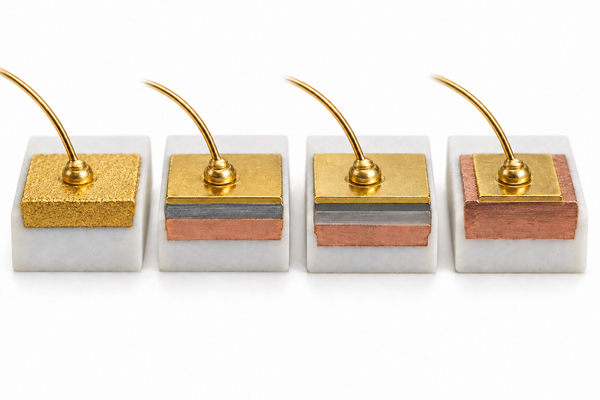
ENIG is primarily selected for solderability and oxidation protection. Its thin immersion-gold layer and exposed nickel behavior after bonding make it a poor default for demanding wire-bond applications unless the exact stack has been qualified. When one surface must support soldering and gold wire bonding, ENEPIG or a selectively plated bond pad is usually a more appropriate evaluation path.
How Do Gold and Aluminum Wire Change the Surface Requirement?
The wire and pad form a metallurgical pair. Compatibility, temperature, ultrasonic energy, and long-term intermetallic behavior matter more than simply matching colors.
| Design choice | Gold wire | Aluminum wire |
|---|---|---|
| Common process | Thermosonic ball bonding or gold wedge bonding | Ultrasonic wedge bonding |
| Typical pad surface | Soft gold or another qualified noble-metal finish | Aluminum or a qualified gold/thick-film system |
| Process temperature | Often uses controlled stage heat | Frequently lower-temperature ultrasonic bonding |
| Main risk to control | Surface contamination, hard or thin gold, excessive intermetallic growth with dissimilar metals | Aluminum oxide, heel damage, pad cratering, and ultrasonic overwork |
| Best specification input | Wire alloy, diameter, ball/stitch geometry, pad finish and heat profile | Wire alloy, diameter, wedge geometry, ultrasonic settings and pad metallurgy |
Copper and silver bonding wires are also used in semiconductor packaging, but they create different force, hardness, oxidation, and reliability requirements. They should not be substituted for gold or aluminum without a separate process qualification.
What Is the Difference Between Ball Bonding and Wedge Bonding?
Ball bonding forms a free-air ball at the wire tip, presses it onto the first pad, creates a controlled loop, and makes a stitch bond at the second pad. It is common with fine gold or copper wire and offers high placement speed. Pad size must accommodate the deformed ball and keep the bond away from conductor edges or fragile underlying features.
Wedge bonding uses a wedge tool and can work with aluminum, gold, or ribbon. It offers low loop profiles and directional control, which can help in RF modules and compact packages. The designer must account for the tool approach direction, wedge footprint, heel area, and clearance along the wire exit path.
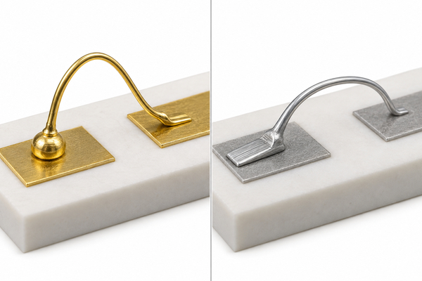
The drawing should state the intended process. A pad that is large enough for a small ball bond may not provide the length or access needed for a wedge bond.
How Should Bond Pads Be Designed on a Ceramic PCB?
Set pad dimensions from the wire diameter, tool footprint, positional tolerance, and required edge margin. Do not apply a generic pad size before the assembly house confirms its capillary or wedge geometry. The drawing should also define the finished pad, not only the underlying conductor artwork.
Keep these design controls explicit:
- Provide a flat, mask-free bond area with no solder, glass overglaze, adhesive, or marking ink.
- Keep the bond impression and wire heel away from pad edges, vias, cavities, conductor neck-downs, and ceramic edges.
- Allow tool access and a clear loop path around die, lids, walls, connectors, and neighboring wires.
- Support thin substrates during bonding and avoid placing critical pads over unsupported cavities.
- Separate bond pads from soldering areas when flux, reflow, or cleaning could contaminate the bond surface.
- Define fiducials and datums that let the assembler locate the die and bond pads consistently.
If the bond layout is dense, provide the bonding diagram with first-bond and second-bond locations, loop direction, wire material, and maximum loop height. This prevents pad design and package geometry from being reviewed as unrelated files.
Which Ceramic PCB Technologies Support Wire Bonding?
Several ceramic circuit processes can create bondable pads, but they do so through different conductor systems and dimensional capabilities.
| Ceramic circuit technology | Why it is considered | Bond-pad planning point |
|---|---|---|
| Thin film | Fine lines, smooth deposited metals, and precise features | Specify adhesion layer, conductor metal, final gold system, and local thickness uniformity |
| DPC | Plated copper thickness with relatively fine features | Define the copper profile and a compatible localized finish over bond pads |
| Thick film | Printed and fired conductors on alumina | Use a wire-bond-qualified gold paste or a validated post-fire plating route |
| HTCC or LTCC | Embedded routing, vias, cavities, and package structures | Coordinate co-fired conductor, braze or plating steps with package sealing and bond sequence |
| DBC or AMB | High-current paths and strong thermal spreading | Reserve suitable bond areas and apply a qualified finish; thick copper alone is not a fine-wire pad specification |
Our thin-film ceramic PCB for wireless communication illustrates the precision-circuit route. For plated copper, a double-sided DPC ceramic circuit for laser equipment shows another relevant platform. Where a power substrate needs a noble-metal finish, a nickel-palladium-gold DBC ceramic PCB is a useful product reference, but its bondability still depends on the final drawing and qualification plan.
For a narrower construction example, see the existing two-layer wire-bondable alumina substrate. That page covers one stack; this guide addresses the broader selection and verification process.
How Do Cleanliness, Roughness, and Plating Quality Affect Bond Strength?
Wire bonding is a solid-state joining process. Oils, fingerprints, photoresist residue, oxides, absorbed organics, glassy paste phases, and particles can prevent intimate metal contact. Cleaning must remove contamination without attacking the finish, changing pad roughness, or leaving ionic residue.
Surface roughness should be controlled rather than assumed to be “as smooth as possible.” A rough or porous surface can reduce the effective contact area and damage fine wire, while an excessively polished or contaminated surface may still produce non-stick defects. Review roughness together with metallization type and the selected bond process.
Plating control includes thickness, purity, hardness, porosity, adhesion, and uniformity across the usable pad. X-ray fluorescence can verify metal thickness, but it does not prove bond performance by itself. Store finished substrates in clean, dry packaging, define shelf life, and avoid touching the pads during inspection and assembly.
What Wire-Bond Failures Should Be Prevented?
Failure analysis should identify where and how the joint failed, not only record the peak force.
| Symptom | Likely contributors | Corrective direction |
|---|---|---|
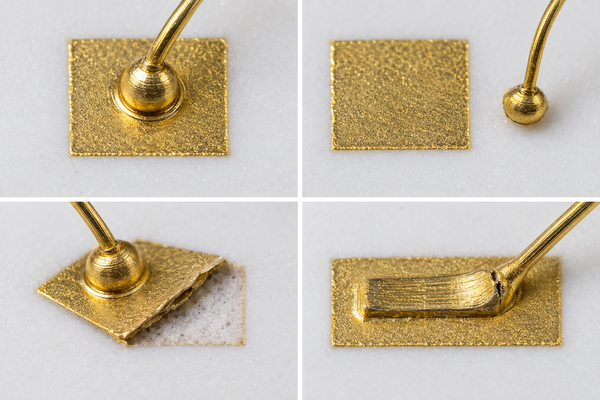
| Non-stick on pad | Contamination, oxide, unsuitable finish, insufficient energy or force | Verify cleaning, surface chemistry, tool condition, and process window |
| Bond lifts from pad | Weak metallurgical interface, hard finish, low energy, poor pad support | Review finish, ultrasonic coupling, stage support, and bond settings |
| Pad or conductor lifts from ceramic | Inadequate metallization adhesion or excessive bond stress | Requalify adhesion, firing or plating sequence, support, and force |
| Heel crack or wire break | Excessive deformation, poor loop geometry, tool wear, work hardening | Adjust loop, force, ultrasonic energy, tool alignment, and wire handling |
| Cratering or ceramic crack | Excessive local stress or unsupported thin substrate | Reduce stress, improve fixture support, move pads, or increase local robustness |
| Early corrosion or resistance drift | Contamination, porous plating, incompatible metals, moisture exposure | Review finish stack, cleanliness, sealing, and environmental qualification |
How Should Wire-Bondable Pads Be Inspected and Qualified?
Use a coupon or production-representative part with the same ceramic, conductor, plating lot, pad geometry, cleaning, storage, wire, tool, and machine settings. A test coupon with a different finish or much larger pads cannot validate the production design.
Qualification normally combines visual inspection, dimensional and plating checks, destructive wire-pull or ball-shear testing, and failure-mode review. Environmental exposure may add thermal cycling, high-temperature storage, humidity, vibration, or other application-specific tests. Acceptance values must be tied to wire diameter, bond type, test geometry, and the chosen standard or customer drawing; one force limit is not valid for every wire and loop.
Process capability is more informative than one passing sample. Record distributions across pads, panels, plating lots, operators, and bonding machines when production risk justifies it.
When Is a Wire-Bondable Finish Unnecessary?
Do not pay for a specialized finish when the substrate will only receive soldered components, pressure contacts, brazed terminals, sintered die attach, or another interconnect that does not use wire bonding. Adding soft gold or ENEPIG without a bonding need can increase cost and introduce an unnecessary controlled interface.
It may also be unnecessary to finish every conductor. Selective bond-pad plating can preserve solderability or high-current copper elsewhere. The drawing should separate bondable pads, solder pads, test contacts, die-attach areas, and protected conductors so each region receives only the required surface treatment.
What Information Should Be Provided to a Ceramic PCB Manufacturer?
Provide enough information to review the substrate and the bonding process together:
- Ceramic material, thickness, outline, flatness, and any cavities or unsupported areas.
- Circuit technology, base conductor, adhesion layer, barrier layer, and final pad finish.
- Wire material, alloy, diameter, ball or wedge method, and intended first/second bond locations.
- Finished pad dimensions, spacing, positional tolerance, keep-outs, and loop-height limits.
- Die size, attach method, package walls, lid or sealing process, and thermal exposures.
- Cleaning restrictions, packaging, shelf-life, and handling requirements.
- Inspection method, plating measurements, sample size, pull or shear test method, and required failure modes.
- Prototype quantity, production volume, drawings, Gerber or CAD data, and assembly sequence.
At BSTCeramicPCB, we can review the ceramic technology, metallization stack, pad layout, and test expectations before fabrication. The most useful starting package includes the substrate drawing and bonding diagram rather than a note that says only “gold pads.”
FAQ
Is every gold-plated ceramic pad wire bondable?
No. Gold thickness, purity, hardness, underlayers, porosity, contamination, and storage all affect the result. The exact finish must be qualified with the intended wire and bond process.
Can ENIG be used for gold wire bonding?
It may bond in some conditions, but it is not the preferred default for demanding gold-wire applications. Evaluate ENEPIG, soft electrolytic gold, fired gold, or selective bond-pad plating against the actual assembly requirements.
Can aluminum wire bond to gold pads?
Qualified aluminum-to-gold systems exist, especially in hybrid circuits, but the material pair and service temperature must be reviewed for intermetallic growth and long-term reliability. Do not approve the combination from material names alone.
Does wire bonding damage ceramic substrates?
A controlled process should not damage a properly designed substrate. Risk increases with thin or unsupported ceramic, weak metallization adhesion, pads near edges or cavities, excessive force, and poor fixture support.
What is the best way to prove bondability?
Build representative coupons or prototypes, bond them with the intended production process, measure pull or shear strength, inspect failure modes, and repeat after the required environmental exposures.
Conclusion
A reliable wire bondable ceramic substrate is defined by a controlled system: ceramic support, conductor adhesion, pad finish, cleanliness, geometry, wire, tool, bonding parameters, and qualification method. Choose the finish only after the assembly process is known, then verify it on production-representative material. To review a ceramic substrate drawing and bonding specification, contact BSTCeramicPCB at sales@bstceramicpcb.com.
 Products
 About us
 Contact us



