






















































 HOME


-

Ceramic PCB for Humanoid Robot joint actuators
2026 04,07 -
LTCC PCB Surprises: What Most People Miss
2025 12,09 -
Step-by-Step Guide to DPC PCB Design for Sensor Systems
2025 12,03 -
Ceramic PCBs Essential Benefits and Applications
2025 12,01 -
How Al2O3 DPC Ceramic Substrate PCB Enhances Heat Dissipation in Modern Electronics?
2025 11,28 -
How to Choose Between Ceramic, FR4, and Metal Core PCBs
2025 11,27 -
DPC Ceramic PCB Materials: Surprising Science Inside
2025 11,26 -
Wire bondable 2-layer Alumina substrates PCB | Bstceramic PCB
2025 09,22 -
Silicon Nitride Substrate, Silicon Nitride Ceramic Substrate Formula
2025 05,08 -
What is thick film ceramic PCB?
2023 08,02
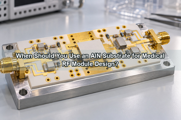
When Should You Use an AlN Substrate for Medical RF Module Design?
Published:
An AlN substrate for medical RF module design can combine electrical insulation, high heat conduction and a stable ceramic platform for RF devices. It is most useful when RF loss, local heat flux, grounding and die or package attachment must be controlled in a compact assembly; it does not by itself certify the finished medical RF system.
What Role Does an AlN Substrate Play in a Medical RF Module?
The AlN substrate can carry power amplifiers, matching networks, switches, filters, control components or bare die while moving heat toward a package base. Patterned conductors, ground structures and vias provide the electrical interconnect. The exact role differs between RF ablation generators, imaging electronics, telemetry modules and other medical equipment.
The substrate is one component inside the RF module. System-level output power, electromagnetic compatibility, patient protection and regulatory compliance remain responsibilities of the module and device manufacturer.
When Is AlN Justified Instead of Alumina or an Organic PCB?
AlN is justified when the ceramic contributes materially to the heat path and the module still requires electrical insulation. Its thermal expansion is relatively close to semiconductor materials, which can also help manage assembly stress. These advantages matter most under concentrated heat sources such as RF power devices.
Alumina may be sufficient for lower heat loads or cost-sensitive designs. An organic RF laminate may offer lower dielectric loss at selected frequencies and is often better for larger, less thermally concentrated routing. Compare the complete electrical, thermal, mechanical and cost requirements rather than treating one material as universally superior.
Which RF Properties Must Be Specified at the Operating Frequency?
Dielectric constant and loss tangent are frequency-, grade- and test-method-dependent. Use data for the selected AlN grade and frequency range, then verify the built transmission structure. A catalog value measured at one frequency should not be silently transferred to another band.
| Input | Why it matters |
|---|---|
| Operating band and bandwidth | Sets the relevant dielectric data and transition design |
| Substrate thickness | Influences impedance geometry and field distribution |
| Metallization thickness and roughness | Affects conductor loss and dimensional compensation |
| Temperature range | Can shift material and device behavior |
| Ground structure | Controls return inductance and mode conversion |
Our thin-film ceramic PCB for wireless communication is a relevant product route when fine RF conductors and precision metallization are central to the design.
How Should Substrate Thickness and Impedance Be Designed?
Choose thickness with the transmission-line structure, target impedance, conductor geometry and assembly strength. A thicker ceramic can require wider lines for the same impedance and can lengthen thermal paths. A thinner ceramic can support compact geometry but may be more sensitive to handling and support conditions.
Do not release only a nominal 50-ohm label. Provide the stack, reference plane, conductor thickness, finish and frequency band. The RF designer should define the target and tolerance; the ceramic manufacturer should confirm the manufacturable geometry and measurement coupon.
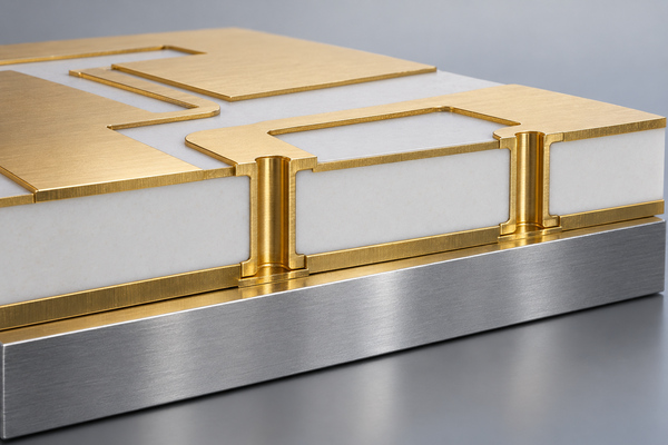
How Do Metallization and Surface Roughness Affect RF Performance?
At higher frequencies, conductor loss becomes sensitive to surface condition and current distribution. The selected DPC or thin-film stack must also support soldering, die attach or wire bonding. These needs can conflict if the top finish and thickness are not defined by pad function.
State finished metal thickness, seed or adhesion system where relevant, top finish, roughness requirement and joining method. Avoid using a generic gold finish for every conductor if only selected pads require a bondable surface.
How Should Grounding and Via Transitions Be Controlled?
RF return paths should be short and continuous. Ground vias around launches, active devices or shield boundaries can reduce return inductance, but spacing and diameter must be evaluated at the operating frequency. A visually dense via fence is not automatically an effective RF transition.
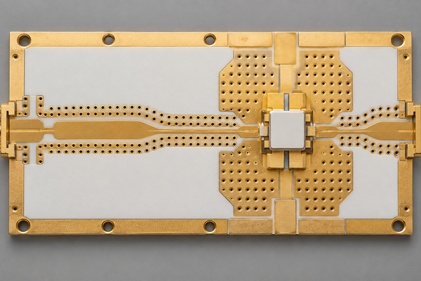
Identify analog, digital, RF and chassis references where the module uses more than one ground domain. The intended join points should be explicit. Thermal copper or package attachment metal should not be assumed to be an RF ground unless the electrical design makes it one.
How Should Heat from RF Power Devices Be Removed?
Map dissipated power at each transistor, MMIC or bias component. The heat path includes die attach, top metal, AlN, lower metal, interface material and the module base. AlN reduces one part of that path, but voids, narrow spreading areas or poor cooler contact can still dominate junction temperature.
Our double-sided AlN DPC ceramic circuit is relevant when the design needs an AlN base with patterned conductors on both faces. The actual RF stack and copper geometry must be reviewed from the customer's files.
What Layout Details Matter Around MMICs, Filters and Matching Networks?
Keep interconnects short, preserve the reference plane and minimize discontinuities at die pads, component pads, vias and connectors. Matching components should be placed according to the RF model, not only mechanical convenience. Reserve bond-tool clearance and probe access without creating long inductive connections.
For bare die, define die-attach pad size, backside grounding, wire-bond length direction and bond-pad finish. For packaged RF devices, include the manufacturer's recommended land pattern and thermal-pad connection, then verify whether it remains appropriate on the ceramic stack.
When Should DPC, Thin Film or LTCC Be Used?
DPC fits patterned copper, plated vias and useful conductor build on ceramic. Thin film is suited to fine, controlled metal geometry and precision bond pads. LTCC supports multilayer routing, cavities and integrated RF structures but uses a different material system and process.
Our LTCC ceramic substrate for power-amplifier circuits is a relevant comparison when the module needs multilayer integration. The process decision should follow RF topology, conductor thickness, line width, vias, cavities and assembly.
How Should Mechanical and Medical-Equipment Boundaries Be Defined?
The drawing should identify substrate support, screw or clamp loads, package sealing, connector forces and thermal-cycle range. If the medical device has a sterilized or patient-contact portion, clarify whether the RF module sits inside or outside that boundary. Do not assign sterilization requirements to the ceramic by assumption.
AlN is brittle like other technical ceramics. Avoid unsupported spans, sharp internal corners and ambiguous edge-chip limits. Package-level stress analysis and thermal cycling should use the actual metal, solder and housing stack.
What Should Be Inspected Before RF Assembly?
Substrate acceptance can include outline, thickness, flatness, conductor registration, line/gap, metal thickness, finish condition, via continuity, isolation and cleanliness. RF-critical coupons may add impedance, insertion loss or transition measurements if the customer defines the structure and method.
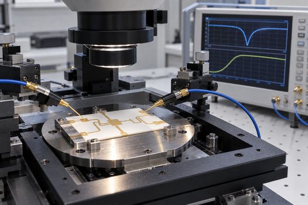
At BSTCeramicPCB, we manufacture the ceramic circuit to the agreed drawing and inspection plan. We do not replace the customer's RF simulation or claim module performance from a bare-substrate check alone.
What Must Be Validated at Module and Device Level?
The assembled RF module should be tested for gain, output power, efficiency, harmonics, noise, stability, thermal behavior and connector or package transitions under its real operating conditions. The medical device team must also address EMC, electrical safety, risk management, software or control behavior and market-specific regulatory requirements.
Use substrate coupons to isolate manufacturing variation, then test the complete module to capture die attach, bonds, components, shielding and enclosure effects. This division keeps component acceptance and system validation clear.
What Information Should You Send Us in the RFQ?
Send us Gerber or ODB++ data, a dimensioned drawing, AlN grade or required properties, substrate thickness, metal stack, finish, vias, critical tolerances and quantities. Add the frequency band, target impedance, stack model, heat sources, die or package attach, wire-bond details, lower interface, inspection coupons and qualification conditions.
Email the files to sales@bstceramicpcb.com. We can review DPC, thin-film or other ceramic process options against the circuit and assembly requirements before quotation.
An AlN substrate for medical RF module design should be selected because the RF, thermal and package requirements support it. Connecting those requirements to the drawing is more valuable than specifying AlN as a material name alone.
 Products
 About us
 Contact us



