






















































 HOME
HOME


-

Ceramic PCB for Humanoid Robot joint actuators
2026 04,07 -
LTCC PCB Surprises: What Most People Miss
2025 12,09 -
Step-by-Step Guide to DPC PCB Design for Sensor Systems
2025 12,03 -
Ceramic PCBs Essential Benefits and Applications
2025 12,01 -
How Al2O3 DPC Ceramic Substrate PCB Enhances Heat Dissipation in Modern Electronics?
2025 11,28 -
How to Choose Between Ceramic, FR4, and Metal Core PCBs
2025 11,27 -
DPC Ceramic PCB Materials: Surprising Science Inside
2025 11,26 -
Wire bondable 2-layer Alumina substrates PCB | Bstceramic PCB
2025 09,22 -
Silicon Nitride Substrate, Silicon Nitride Ceramic Substrate Formula
2025 05,08 -
What is thick film ceramic PCB?
2023 08,02
Alumina PCB Manufacturer: Processes, Capabilities and Quality Control
Published:
An alumina PCB manufacturer converts an electrically insulating Al2O3 ceramic substrate into a functional circuit by combining substrate preparation, metallization, patterning, surface finishing, singulation, inspection, and, when required, component assembly. The result may be a fine-line DPC circuit, a heavy-copper DBC board, a printed thick-film hybrid, or a precision thin-film structure. These processes use the same ceramic family, but they do not have the same design rules or performance limits.
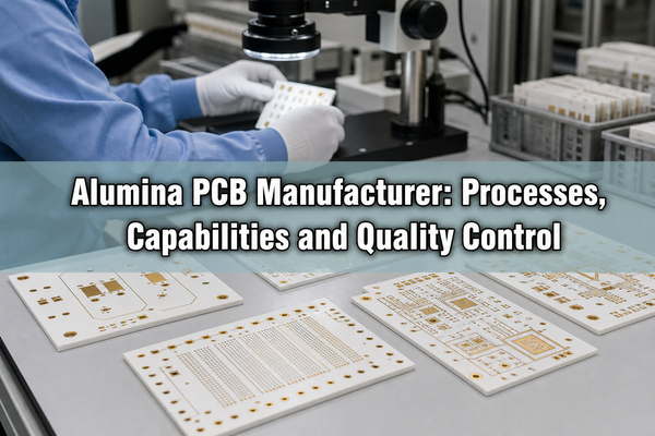
Alumina is widely used because it provides electrical insulation, useful thermal conductivity, dimensional stability, and a mature manufacturing base at a lower material cost than aluminum nitride. Its practical performance still depends on purity, thickness, surface condition, conductor system, copper geometry, and the complete thermal path. This guide explains how those choices affect a manufacturable alumina circuit board.
What Does an Alumina PCB Manufacturer Make?
An alumina PCB board is more than a fired white ceramic sheet. The finished structure combines an alumina substrate with conductors, pads, resistors or other functional films, protective layers, and a termination system suitable for soldering, brazing, wire bonding, or direct device attachment. Depending on the design, the circuit can be single-sided, double-sided, interconnected through metallized holes, or built as a hybrid multilayer structure.
A ceramic PCB manufacturer must therefore control both ceramic behavior and circuit fabrication. The ceramic is hard and electrically stable but brittle. The metal must adhere to the surface, maintain the required geometry, survive thermal cycling, and remain compatible with the selected assembly process. A layout that is straightforward on FR4 may require different edge clearances, corner radii, hole methods, and panel handling on an alumina ceramic PCB.
The manufacturing output can include bare ceramic circuits, resistor networks, power-device substrates, LED submounts, sensor circuits, and assembled modules. The process route is selected according to conductor thickness, feature size, thermal load, operating temperature, surface finish, and interconnection method rather than by the alumina material name alone.
Why Is Alumina Used as a PCB Substrate?
Alumina is an electrical insulator that conducts heat far better than common organic laminates. This allows copper, silver, gold, or other compatible metallization to sit directly on the ceramic without a separate low-conductivity polymer dielectric between the circuit and the supporting substrate. The shorter thermal path is useful for compact power devices, LEDs, sensors, and hybrid circuits.
Dense alumina also provides high dielectric strength, low moisture absorption, good chemical stability, and useful mechanical rigidity. Its coefficient of thermal expansion is lower than copper and closer to many semiconductor and glass materials than an aluminum metal core. That can reduce, but not eliminate, stress in die-attach and solder joints.
The term ceramic circuit board material is still too broad to define performance. Alumina purity, grain structure, density, thickness, surface roughness, and test temperature affect thermal, dielectric, and mechanical results. A published conductivity or strength value should be treated as grade-specific data, not as a universal property of every alumina PCB substrate.
Which Alumina Grades Are Used for PCB Manufacturing?
Commercial electronic substrates commonly use alumina in the range from about 92% to 99.6% purity, with 96% and 99.6% being frequent reference grades. The balance is not empty space; it consists of glassy or mineral additives that assist sintering and influence surface, dielectric, thermal, and mechanical behavior.
| Grade | Typical reason for use | Manufacturing consideration |
|---|---|---|
| 92% to 96% Al2O3 | Mature availability, practical cost, good insulation, and compatibility with many thick-film and DPC systems | The glassy phase and surface condition must match the selected metallization and firing profile |
| 99% Al2O3 | Higher purity where dielectric loss, chemical stability, or surface consistency is more demanding | Material availability and process windows are more grade-specific than for common 96% substrates |
| 99.6% Al2O3 | High-purity circuits, thin-film metallization, wire bonding, and applications requiring controlled surface or electrical behavior | Higher material cost is justified only when the design benefits from the tighter material characteristics |
Higher purity does not automatically make a better circuit. A 96% substrate can be the more appropriate option when the metallization system, mechanical dimensions, thermal load, and cost target are already satisfied. The detailed comparison of 96% and 99.6% alumina substrates shows why surface quality and process compatibility can matter more than purity alone.
Which Manufacturing Processes Are Available for Alumina PCBs?
Alumina supports several metallization routes. Each route creates the conductor in a different way, so feature size, copper thickness, adhesion mechanism, resistor integration, and thermal behavior must be evaluated together.
- DPC builds copper through seed-layer deposition, photolithography, electroplating, and pattern definition. It suits fine features and controlled plated copper thickness.
- DBC bonds copper foil directly to ceramic at high temperature and then patterns the copper. It suits power circuits that need substantially thicker copper and strong heat spreading.
- Thick-film processing screen-prints conductor, resistor, dielectric, or protective pastes and fires them onto the ceramic. It supports integrated resistors and hybrid circuit functions.
- Thin-film processing deposits very thin metal layers by vacuum techniques and defines precision features through photolithography and etching or lift-off.
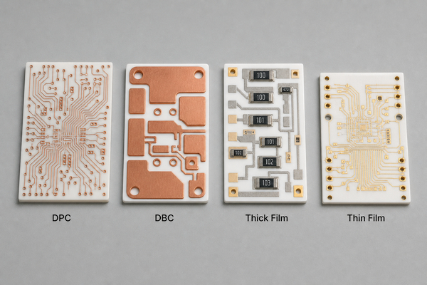
Processes can sometimes be combined, but they should not be mixed casually. Paste firing temperature, copper oxidation control, seed-layer adhesion, ceramic surface roughness, and later plating or assembly steps must remain chemically and mechanically compatible.
How Do DPC, DBC, Thick-Film and Thin-Film Alumina PCBs Differ?
The practical selection begins with conductor thickness and feature size. Heavy current and lateral heat spreading favor thick copper; dense signal routing and small pads favor photolithographic precision; integrated resistors favor printable functional pastes.
| Process | Conductor structure | Best fit | Primary constraint |
|---|---|---|---|
| DPC | Plated copper formed over a deposited seed layer | Fine-line ceramic circuits, vias, sensor and optoelectronic layouts, moderate copper thickness | Plating uniformity, seed-layer adhesion, and current distribution affect final copper geometry |
| DBC | Relatively thick copper foil bonded directly to alumina and etched | Power modules, high-current paths, large thermal pads, and copper-clad alumina PCB structures | Fine spacing is limited by copper thickness and etching; copper area can add thermal-mechanical stress |
| Thick film | Fired conductor and resistor pastes printed on ceramic | Hybrid circuits, printed resistors, heaters, sensors, high-temperature functional layers | Printed resolution, fired thickness, paste resistance, and firing compatibility define the process window |
| Thin film | Vacuum-deposited metal layers patterned with high-resolution lithography | Microwave, optical, medical, and precision thin film alumina ceramic PCB structures | Very thin conductors are not a substitute for heavy-current copper; surface quality is critical |
A DPC circuit and a DBC circuit may both use copper on alumina, but they solve different problems. More detail is available in the site guides to DPC ceramic PCB and DBC ceramic PCB.
How Is an Alumina PCB Manufactured?
The process starts with a released alumina grade and substrate thickness. The ceramic surface is cleaned, inspected, and prepared for the chosen metallization. Laser drilling, mechanical drilling, punching, or pre-fired features may be used for holes and slots, but the method depends on thickness, feature geometry, edge-quality requirement, and production route.
DPC manufacturing typically applies an adhesion or seed layer, coats photoresist, exposes the circuit image, plates copper to the required build, removes the resist, and etches unwanted seed material. DBC begins with copper foil bonding under a controlled high-temperature atmosphere, followed by imaging and copper etching. Thick-film circuits are printed, dried, fired, and repeated for additional conductor, resistor, dielectric, or overglaze layers. Thin-film circuits use controlled deposition and lithography to form much finer metal structures.
After metallization, the panel may receive nickel, gold, silver, tin, or another compatible finish. Laser scribing, laser cutting, grinding, or dicing separates the finished parts. Cleaning, dimensional inspection, electrical testing, adhesion evaluation, surface inspection, and packaging follow according to the released process.
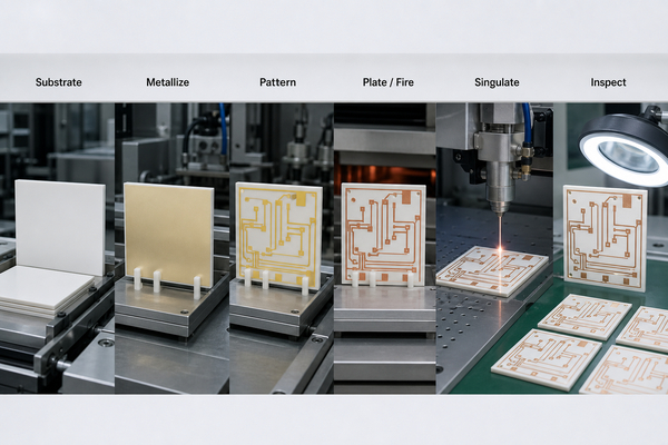
For printed conductors and resistive features, thick-film ceramic PCB manufacturing uses a different sequence and material system from plated copper. Screen design, paste rheology, drying, firing atmosphere, layer registration, and resistance trimming all influence the finished circuit.
How Do Substrate Thickness and Copper Thickness Affect the Build?
Substrate thickness affects mechanical rigidity, thermal resistance through the ceramic, dielectric spacing, hole aspect, and the risk of breakage during processing. A thinner ceramic shortens the through-thickness heat path and reduces package height, but large thin panels are more sensitive to handling, flatness, local clamping, and singulation damage.
Copper thickness affects current capacity, lateral heat spreading, etch geometry, minimum spacing, and thermal stress. Thick copper is useful for power circuits, but the sidewall undercut of an etched conductor grows with copper thickness. Large asymmetric copper areas can also pull on the ceramic during temperature changes because copper expands more than alumina.
The two thicknesses should be selected together. A very thick, unbalanced copper pattern on a thin alumina sheet may create bow or cycling stress even if the electrical design is acceptable. Symmetric copper distribution, rounded transitions, divided thermal pads, and controlled copper-to-edge distance can reduce stress concentration.
Which Design Rules Affect Alumina PCB Manufacturability?
Ceramic layouts should use the design rules of the selected process, not copied FR4 limits. DPC, DBC, thick-film, and thin-film lines have different minimum features, registration behavior, conductor thickness, via structures, and edge quality.
- Use generous internal corner radii in ceramic outlines, slots, and cutouts to reduce crack initiation.
- Keep copper, pads, and fired films away from scored or laser-cut edges according to the process-specific margin.
- Avoid narrow ceramic bridges between holes, slots, and the board edge.
- Balance large copper regions where possible and avoid abrupt thick-to-thin conductor transitions.
- Define whether holes are metallized, non-plated, laser-drilled, mechanically drilled, or formed before firing.
- Place wire-bond pads, solder pads, and brazed terminals according to the finish, flatness, cleanliness, and assembly method they require.
A manufacturer may be able to make a small isolated feature on a test coupon but not repeat it economically across a large panel with the required yield. Manufacturability therefore includes registration, handling, inspection access, singulation, and process capability across the full production layout.
Which Surface Finishes and Assembly Options Are Available?
The surface finish must match the base metallization and the intended interconnection. Copper circuits may use nickel/gold systems, immersion finishes, silver, or other released coatings for solderability, corrosion protection, wire bonding, or die attachment. Thick-film silver, silver-palladium, gold, or other paste systems require finish combinations compatible with the fired conductor and service environment.
Assembly can include SMT soldering, reflow, wire bonding, die attach, brazed terminals, conductive adhesive, and ceramic PCB assembly. The ceramic's higher heat transfer and thermal mass can change reflow heating and cooling compared with FR4. Large ceramic-to-metal joints should be evaluated for CTE mismatch and temperature gradients instead of relying on a standard profile without verification.
Solder mask and protective coatings are process-dependent. Organic solder mask may be suitable for some copper circuits, while glass-based overglaze or dielectric layers are used where higher temperature or compatibility with printed functional films is required. No single finish stack is correct for every alumina circuit board.
How Are Alumina PCBs Inspected and Tested?
Inspection begins with the ceramic itself. Thickness, dimensions, flatness, edge condition, hole geometry, surface contamination, and visible cracks can affect every later step. After metallization, line width, spacing, copper or film thickness, registration, pad geometry, finish coverage, and surface defects are checked against the released drawing and process plan.
| Control area | Typical verification | Why it matters |
|---|---|---|
| Substrate | Dimensions, thickness, flatness, surface and edge inspection | Prevents poor registration, assembly gaps, and crack propagation |
| Metallization | Thickness measurement, optical inspection, adhesion or peel evaluation where applicable | Confirms conductor geometry and bond integrity |
| Electrical circuit | Continuity, isolation, resistance, flying-probe or fixture testing | Detects opens, shorts, incorrect networks, and leakage paths |
| Interconnection | Via continuity, cross-section analysis, solderability or bondability checks | Verifies hidden interfaces and assembly readiness |
| Reliability | Thermal cycling, high-temperature storage, dielectric or environmental tests when specified | Reveals stress, adhesion, finish, and insulation changes over time |
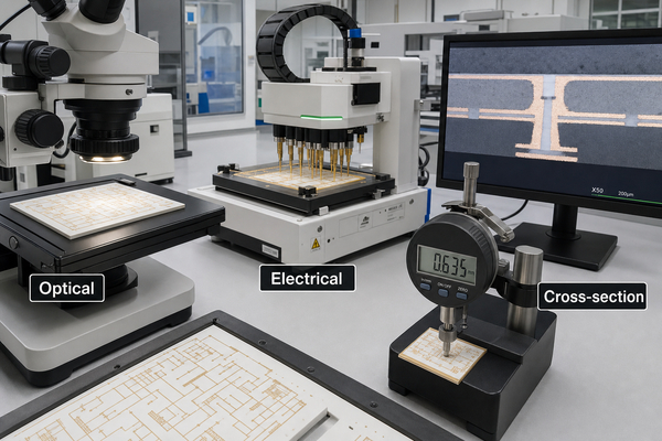
BSTCeramicPCB uses staged controls from substrate inspection through circuit and final verification. The site overview of ceramic PCB inspection and testing describes electrical, dimensional, metallographic, solderability, and related quality checks used for released ceramic circuit processes.
Which Applications Use Alumina PCBs?
Alumina circuits are useful where an organic laminate would add excessive thermal resistance, dimensional movement, moisture uptake, or temperature limitation. Typical applications include:
- LED modules and laser-diode submounts that need a short thermal path and electrical isolation.
- Automotive sensors, fuel-level circuits, ignition electronics, and compact control modules exposed to heat and vibration.
- Power devices, converters, and industrial controls using DBC or DPC copper structures.
- Medical analyzers, imaging electronics, fluid-control devices, and precision sensor modules.
- RF, microwave, optoelectronic, and wire-bonded circuits using controlled surfaces and fine features.
- Printed heaters, resistor networks, and high-temperature hybrid circuits made with thick-film materials.
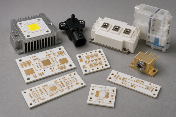
Alumina is not automatically necessary for every hot component. FR4, insulated metal substrate, flex, or aluminum nitride may be more appropriate when routing density, flexibility, cost, very high heat flux, or assembly architecture dominates the design.
What Are the Main Manufacturing Limits of Alumina PCBs?
The first limit is brittleness. Alumina tolerates compression well but is sensitive to impact, edge defects, point loading, and tensile stress. Large thin boards, narrow bridges, sharp internal corners, and force-fit fasteners increase breakage risk.
The second limit is process-specific geometry. Thick copper cannot be etched with the same fine spacing as a thin plated layer. Screen-printed films cannot reproduce every thin-film feature. Thin-film conductors cannot carry the same current as DBC copper. The board must be designed for the selected metallization route.
The third limit is thermal-mechanical mismatch. Copper, solder, attached components, heat sinks, and housings expand differently from Al2O3 ceramic. Large continuous copper areas or rigid mounts can transfer that strain into the ceramic and joints during cycling. Balanced metal, compliant attachment, controlled ramp rates, and suitable joint geometry reduce this risk.
Finally, nominal material data does not describe the complete assembly. Ceramic thickness, metal area, interface layers, surface finish, die attach, airflow, and heat-sink contact can change junction temperature and reliability more than a small difference between two alumina data sheets.
FAQ About Alumina PCB Manufacturing
Can alumina PCBs pass SMT reflow?
Yes, alumina circuits can support SMT assembly when the metallization, finish, solder paste, component terminations, and profile are compatible. The ceramic may heat and cool differently from FR4, so thermal gradients, board support, component mass, and cooling rate should be verified on the actual assembly.
Can alumina PCBs be multilayer?
Multilayer ceramic circuits are possible through thick-film dielectric/conductor stacks, plated interconnections, or co-fired ceramic technologies. The achievable layer count and feature rules depend on the process. A multilayer thick-film hybrid is not built like a laminated FR4 multilayer PCB.
Is 96% alumina suitable for every PCB?
No. It is a practical and widely used grade, but high-purity alumina may be preferred for tighter dielectric, surface, loss, or thin-film requirements. Aluminum nitride may be more suitable where the heat flux and temperature-uniformity target exceed what the complete alumina structure can provide.
Is an alumina PCB the same as an aluminum PCB?
No. An alumina PCB uses electrically insulating aluminum oxide ceramic as the substrate. An aluminum PCB normally uses a metallic aluminum base separated from the copper circuit by a polymer dielectric. Their thermal path, electrical structure, drilling, routing, and failure modes are different.
Can DPC and DBC use the same design rules?
No. DPC builds plated copper and is suited to finer features, while DBC starts with much thicker bonded copper and needs etch geometry and stress control appropriate to that copper thickness. Pad size, line spacing, copper balance, edge distance, and via options must follow the selected process.
Conclusion
A capable alumina PCB manufacturer must match the substrate grade, metallization process, copper or film thickness, feature geometry, surface finish, assembly method, and inspection plan as one manufacturing system. DPC supports plated fine-line copper, DBC supports heavy copper power structures, thick film integrates printed conductors and resistors, and thin film supports precision metal patterns. None is universally best.
BSTCeramicPCB supports alumina ceramic circuits through multiple released ceramic PCB processes and staged quality control. For a technical discussion about an alumina circuit structure, contact sales@bstceramicpcb.com.
 Products
 About us
 Contact us



