






















































 HOME
HOME

-

Ceramic PCB for Humanoid Robot joint actuators
2026 04,07 -
LTCC PCB Surprises: What Most People Miss
2025 12,09 -
Step-by-Step Guide to DPC PCB Design for Sensor Systems
2025 12,03 -
Ceramic PCBs Essential Benefits and Applications
2025 12,01 -
How Al2O3 DPC Ceramic Substrate PCB Enhances Heat Dissipation in Modern Electronics?
2025 11,28 -
How to Choose Between Ceramic, FR4, and Metal Core PCBs
2025 11,27 -
DPC Ceramic PCB Materials: Surprising Science Inside
2025 11,26 -
Wire bondable 2-layer Alumina substrates PCB | Bstceramic PCB
2025 09,22 -
Silicon Nitride Substrate, Silicon Nitride Ceramic Substrate Formula
2025 05,08 -
What is thick film ceramic PCB?
2023 08,02
Ceramic Electricity Conductor or Insulator: PCB Material Guide
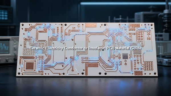
Ceramic electricity conductor or insulator is not a single yes-or-no material category. Most alumina, aluminum nitride, and silicon nitride PCB substrates are electrical insulators, while some specialized ceramics are semiconductive, electronically conductive, or ionically conductive. A ceramic PCB works by combining an insulating ceramic body with deliberately patterned metal conductors, vias, and terminals.
Is Ceramic an Electrical Conductor or Insulator?
Most technical ceramics used as PCB substrates are electrical insulators under their specified operating conditions. They contain very few mobile electrons, so current does not flow through the bulk material as it does through copper or aluminum.
The word ceramic covers many chemistries and structures, however. Silicon carbide can be semiconductive, certain oxide ceramics can conduct electrons, and solid electrolytes can conduct ions. The correct answer must therefore identify the ceramic composition, temperature, electric field, frequency, and measurement direction.
Why Are Most Technical Ceramics Electrical Insulators?
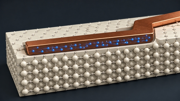
Most oxide and nitride substrate ceramics have strong ionic and covalent bonds that hold electrons in place. Their electronic band structure creates a large energy barrier between occupied and mobile electronic states, so ordinary operating voltages do not produce metal-like conduction.
Dense 99% alumina and selected AlN grades can have published room-temperature volume resistivity above 10^14 Ω·cm. That figure is a grade-specific example, not a universal ceramic value. Pores, additives, surface films, contamination, humidity, temperature, and test method can change the measured resistance substantially.
Which Ceramics Can Conduct Electricity?
Some ceramics conduct electricity through electrons, holes, or mobile ions. Conductive or semiconductive examples include selected silicon carbide compositions, titanium-based oxides, ruthenium oxide resistor materials, and engineered zirconia grades used for electrostatic-dissipative behavior. Solid electrolytes conduct ions rather than carrying electronic circuit current like copper.
Composition is not enough by itself. Dopants, oxidation state, grain boundaries, temperature, atmosphere, and electrode contact can change the conduction mechanism. A material described as a conductive ceramic should therefore not be substituted for an insulating PCB substrate without electrical and reliability validation.
Resistivity, Dielectric Strength and Dielectric Constant Are Different
These electrical parameters describe different behavior and should not be used interchangeably.
| Parameter | What it describes | Why it matters on a ceramic PCB |
|---|---|---|
| Volume resistivity | Resistance through the bulk material | Bulk leakage and isolation |
| Surface resistivity | Resistance along the ceramic surface | Sensitivity to moisture and contamination |
| Dielectric strength | Electric field that causes breakdown under a stated test | Minimum thickness and high-voltage margin |
| Dielectric constant | Electric-field storage relative to vacuum | Capacitance, impedance and RF behavior |
| Dielectric loss | Energy dissipated in an alternating electric field | RF loss and heating |
An insulator still has finite resistance and can fail if the electric field is high enough. A high dielectric constant does not mean high conductivity, and a high room-temperature resistivity does not guarantee safe isolation at elevated temperature.
How Do Alumina, AlN and Si3N4 Compare Electrically?
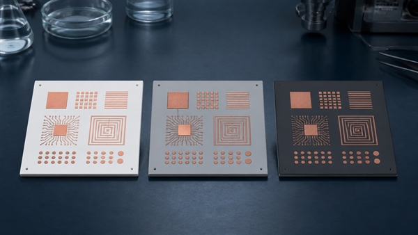
Alumina, aluminum nitride, and silicon nitride are normally used as electrically insulating substrates, but their thermal and mechanical behavior differs.
| Substrate | Electrical role | Main engineering distinction |
|---|---|---|
| Alumina (Al2O3) | Insulating | Mature, versatile, available in multiple purities and processes |
| Aluminum nitride (AlN) | Insulating | Much higher thermal conductivity than common alumina grades |
| Silicon nitride (Si3N4) | Insulating | High fracture toughness and strong thermal-shock capability |
The final choice must use the actual grade datasheet because purity, additives, density, surface finish, and temperature affect electrical properties. The BSTCeramicPCB comparison of common ceramic circuit board materials provides the broader thermal and mechanical context.
How Does Metallization Make a Ceramic PCB Conductive?
Metallization creates controlled current paths on or through an insulating ceramic substrate. Copper, silver, gold, tungsten, molybdenum, or other compatible conductor systems are patterned according to the manufacturing process. The ceramic separates traces and provides mechanical support, while the metal carries current.
A fine-feature alumina DPC ceramic substrate PCB for LED applications builds metal on an insulating Al2O3 surface. The board is conductive only along the designed metal network; exposed ceramic between traces remains the dielectric isolation region.
How Do DPC, Thick Film, DBC, AMB, LTCC and HTCC Carry Current?
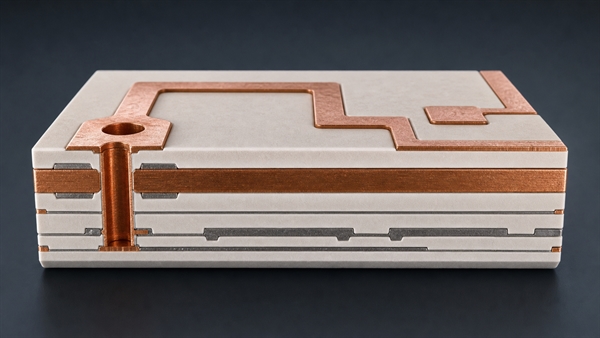
Each ceramic PCB process forms its conductor differently, so line geometry, metal thickness, adhesion, current capacity, and temperature limit must be reviewed process by process.
- DPC: deposits and plates patterned copper for fine features and plated vias.
- Thick film: screen-prints and fires conductor pastes on ceramic.
- DBC: bonds relatively thick copper foil directly to an oxide ceramic interface.
- AMB: uses an active-metal braze to bond copper to ceramics such as Si3N4.
- LTCC: co-fires ceramic tapes and compatible internal conductors at a lower ceramic firing temperature.
- HTCC: co-fires refractory-metal conductors with high-temperature ceramic systems.
An AlN DPC ceramic substrate for a stabilizer and an LTCC ceramic substrate PCB for vehicle electronics can both route current while isolating circuits, but their metal systems, layer construction, feature limits, and thermal paths are different. See the BSTCeramicPCB guide to ceramic PCB metallization processes for more process detail.
How Do Temperature, Moisture and Purity Change Insulation?
Electrical resistance often decreases as temperature rises because more charge carriers can move through defects, grain boundaries, or secondary phases. Moisture and ionic contamination can create a conductive surface film even when the bulk ceramic remains highly resistive.
Lower-purity alumina may contain more glassy or additive-rich grain-boundary phases. These are useful for sintering but can change dielectric loss, resistivity, and high-temperature behavior. Design values should therefore come from the specified grade at the intended temperature and frequency, not from a generic room-temperature material table.
How Do Creepage, Clearance and Surface Cleanliness Prevent Breakdown?
Creepage, clearance, geometry, and cleanliness determine whether a high-resistivity ceramic actually provides reliable circuit isolation. Sharp conductor corners concentrate electric field, small spacing reduces margin, and contamination can create leakage paths along the surface.
Review the maximum working and transient voltage, altitude, environment, coating, ceramic thickness, conductor edge shape, via-to-trace spacing, and expected contamination level. Critical assemblies may require insulation-resistance testing, dielectric-withstand testing, partial-discharge evaluation, or thermal-humidity bias testing under application-specific conditions.
How Should a Ceramic PCB Material Be Selected for Electrical Isolation?
Select the ceramic and metallization as one system. The substrate must provide the required isolation while the conductor process must carry current, remove heat, survive assembly, and maintain adhesion during thermal cycling.
Check these items together:
- volume and surface resistivity at operating temperature;
- dielectric strength, thickness, creepage, and clearance;
- dielectric constant and loss at the circuit frequency;
- thermal conductivity and coefficient of thermal expansion;
- fracture toughness, flexural strength, and edge quality;
- conductor metal, thickness, width, via structure, and surface finish;
- metallization adhesion and thermal-cycle reliability;
- cleaning, coating, sealing, and environmental exposure.
Frequently Asked Questions
1. Are ceramics electrical conductors or insulators?
Most common substrate ceramics are electrical insulators, but some engineered ceramics are conductive, semiconductive, or ionically conductive. Always identify the specific composition and test condition.
2. Is ceramic a good electrical insulator?
Dense alumina, AlN, and Si3N4 can provide strong electrical insulation, heat resistance, and dimensional stability. Their suitability still depends on voltage, temperature, frequency, thickness, surface condition, and the actual grade data.
3. Does a ceramic insulator conduct any current?
Every real insulator has finite resistance, so a very small leakage current can exist. Leakage increases with temperature, moisture, contamination, defects, and electric field, and breakdown occurs if the material limit is exceeded.
4. Is ceramic also a thermal insulator?
Electrical and thermal conduction are different. Many electrical-insulating ceramics conduct heat better than polymer dielectrics; AlN is a key example. Do not infer thermal behavior from electrical insulation alone.
Conclusion
Ceramic electricity conductor or insulator should be answered at the material and circuit-system levels. Most ceramic PCB substrates insulate, while patterned metal layers and vias carry current; specialized ceramics can also be conductive or semiconductive. For substrate, metallization, spacing, and reliability review, contact BSTCeramicPCB at sales@bstceramicpcb.com.
 Products
 About us
 Contact us



