






















































 HOME
HOME


-

Ceramic PCB for Humanoid Robot joint actuators
2026 04,07 -
LTCC PCB Surprises: What Most People Miss
2025 12,09 -
Step-by-Step Guide to DPC PCB Design for Sensor Systems
2025 12,03 -
Ceramic PCBs Essential Benefits and Applications
2025 12,01 -
How Al2O3 DPC Ceramic Substrate PCB Enhances Heat Dissipation in Modern Electronics?
2025 11,28 -
How to Choose Between Ceramic, FR4, and Metal Core PCBs
2025 11,27 -
DPC Ceramic PCB Materials: Surprising Science Inside
2025 11,26 -
Wire bondable 2-layer Alumina substrates PCB | Bstceramic PCB
2025 09,22 -
Silicon Nitride Substrate, Silicon Nitride Ceramic Substrate Formula
2025 05,08 -
What is thick film ceramic PCB?
2023 08,02
Ceramic PCB Applications in LEDs, IGBT Modules and Power Electronics
Published:
Ceramic PCB applications in LEDs, IGBT modules and power electronics are driven by one requirement: move heat through an electrically insulating structure without losing circuit reliability. The ceramic board may also carry current, support bare dies, provide wire-bond surfaces and survive repeated temperature changes. Ceramic is therefore justified when the complete thermal, electrical and mechanical stack exceeds what FR4 or a conventional metal-core PCB can support. It is unnecessary when a lower-cost board already keeps junction temperature, voltage stress and assembly reliability within specification.
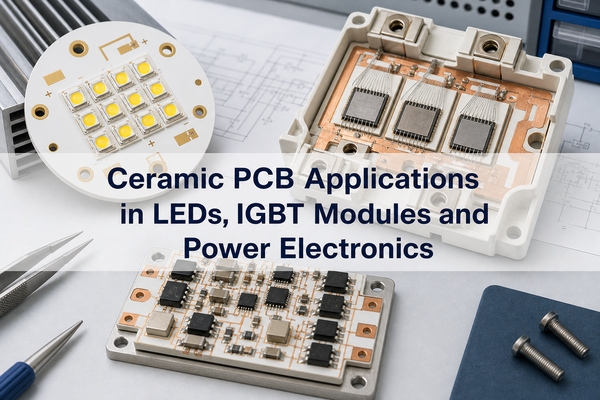
Why Are Ceramic PCBs Used in LEDs, IGBT Modules and Power Electronics?
Ceramic PCBs combine electrical insulation with a direct heat-transfer path. Unlike an insulated metal substrate, a metallized ceramic board does not require a thick polymer dielectric between the circuit and the cooling surface. That difference becomes valuable when heat flux is concentrated under an LED die or power semiconductor, when isolation voltage is high, or when repeated thermal cycling makes polymer interfaces the reliability limit.
| Application load | What the ceramic PCB contributes | Selection boundary |
|---|---|---|
| Concentrated LED heat | Short thermal path, stable mounting surface and electrical isolation | Use ceramic only if junction-temperature analysis shows FR4 or MCPCB is insufficient |
| IGBT or MOSFET switching loss | Heat spreading, die support, high-current copper and isolation from the cooler | Copper thickness, pattern geometry and partial-discharge performance must be considered together |
| Repeated power cycling | Low expansion, stable dielectric behavior and controlled copper-to-ceramic attachment | Material strength and copper balance may matter more than maximum thermal conductivity |
| High-voltage conversion | Thin insulating layer with useful heat transfer | Creepage, clearance, edge condition and test voltage remain design-specific |
The practical decision is not "ceramic or no ceramic" in isolation. It is whether a particular ceramic, copper process and assembly stack can meet the temperature, voltage and lifetime target with acceptable manufacturing margin.
How Do Ceramic PCBs Work in High-Power LED Applications?
A ceramic PCB for LED applications conducts heat from the LED package or bare die into a heat spreader while keeping the electrical circuit isolated. The useful metric is not substrate thermal conductivity alone. Engineers should estimate the complete path from junction to die attach, metallization, ceramic, thermal interface material and heat sink. A high-conductivity substrate cannot compensate for a voided solder layer or an undersized heat sink.
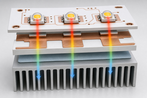
| LED use case | Practical ceramic option | Critical check |
|---|---|---|
| High-brightness lighting module | Alumina DPC where cost and moderate heat flux dominate | LED junction temperature at maximum ambient and drive current |
| UV-C LED or compact high-flux array | AlN DPC when the substrate is a meaningful part of total thermal resistance | Delivered AlN thermal-conductivity grade and metallization adhesion |
| Automotive headlamp | Alumina or AlN selected from heat flux, footprint and cycling requirement | Solder fatigue, thermal shock, vibration and optical output stability |
| COB or multi-die LED | DPC or thin-film structure for controlled die pads and wire bonding | Pad flatness, die-attach coverage, finish and wire-bond pull strength |
An alumina DPC ceramic PCB for LED modules is a sensible starting point when the design needs defined copper features and a direct ceramic heat path but does not require the higher cost of AlN. AlN becomes worthwhile when thermal simulation or prototype measurements show that alumina is the limiting layer. For low-power lamps with a large board area, an MCPCB may remain the more economical solution.
How Are Ceramic PCBs Used in IGBT Modules?
In an IGBT module, the ceramic substrate sits between semiconductor dies and the cooler or baseplate. It must conduct switching and conduction heat, route high current, isolate high voltage and support die attach and wire bonds. These functions make substrate selection part of package design, not a simple PCB material substitution.
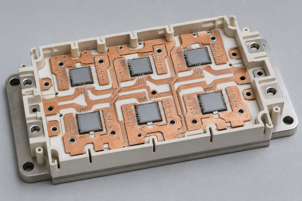
DBC and AMB are common choices because they attach substantial copper to ceramic. A DBC ceramic substrate for an IGBT module fits many industrial modules where current capacity, insulation and thermal transfer are the main drivers. An AMB ceramic PCB for IGBT power cycling is often considered when a silicon nitride substrate and stronger mechanical reliability are needed for severe cycling or automotive duty.
| Decision factor | DBC path | AMB path |
|---|---|---|
| Typical ceramic pairing | Alumina or AlN | Commonly silicon nitride for high-reliability modules |
| Main strength | Established thick-copper power substrate with effective heat spreading | Strong copper-to-ceramic system for demanding thermal and mechanical cycling |
| Suitable starting point | Industrial drives, converters, conventional IGBT power modules | EV traction, SiC power modules and applications with aggressive lifetime targets |
| Engineering caution | Copper thickness and pattern balance can increase stress and bow | Brazing system, ceramic grade and process control must be qualified as one construction |
Neither process should be selected from device current alone. Switching loss distribution, die size, junction-temperature swing, busbar geometry, commutation-loop inductance, cooler flatness and solder or sinter attachment all affect module performance.
Where Are Ceramic PCBs Used in Other Power Electronics?
Ceramic PCBs are used where power conversion creates concentrated heat while the circuit still needs electrical isolation. The same substrate concept appears in traction inverters, onboard chargers, industrial motor drives, renewable-energy converters, UPS systems, welding power supplies and compact DC-DC modules, but the correct construction changes with the load profile.
| Power-electronics system | Dominant requirement | Likely starting point |
|---|---|---|
| EV traction inverter | High current, rapid cycling and long lifetime | Si3N4 AMB or another qualified high-reliability power substrate |
| Industrial motor drive | Continuous load, isolation and service life | Alumina or AlN DBC, depending on heat flux |
| Solar or energy-storage inverter | Repeated daily cycling and outdoor temperature range | DBC or AMB after power-cycling analysis |
| Compact DC-DC converter | Small footprint and concentrated loss | DPC for finer geometry or DBC for higher current |
| Power supply or heater control | Moderate geometry with printed resistive functions | Thick film when integrated resistors and cost are more important than heavy copper |
A ceramic PCB for power electronics should be selected against the hottest operating point and the most damaging cycle, not only nominal power. A 24-hour steady industrial supply and an automotive inverter with rapid torque changes can require different substrates even when their average power is similar.
Which Ceramic Material Fits Each Application?
Ceramic PCB materials should be compared as part of a stack. Representative supplier data commonly places alumina near 20-30 W/mK, AlN around 170 W/mK and power-substrate Si3N4 around 90 W/mK, but actual values depend on grade, purity, temperature and measurement method. These figures are selection ranges, not guaranteed board performance.
| Material | Best fit | Main advantage | Main trade-off |
|---|---|---|---|
| Alumina (Al2O3) | Cost-sensitive LEDs, industrial power and established DBC designs | Economical, electrically insulating and widely available | Lower thermal conductivity and lower fracture toughness than specialized alternatives |
| Aluminum nitride (AlN) | High-flux LEDs, laser devices and compact power modules | High thermal conductivity with expansion closer to semiconductor materials | Higher cost; delivered grade and moisture-sensitive processing history require control |
| Silicon nitride (Si3N4) | EV, SiC and severe power-cycling modules | High strength and fracture toughness with useful thermal conductivity | Higher material and AMB process cost; selected for lifetime rather than peak conductivity |
Material selection should start from the thermal-resistance budget and reliability load. Alumina is often adequate when the ceramic is not the dominant thermal bottleneck. AlN is valuable when reducing substrate thermal resistance changes junction temperature meaningfully. Si3N4 is compelling when crack resistance and thermal cycling dominate the lifetime model.
Which Metallization Process Should Be Used?
The metallization process determines copper thickness, pattern resolution, bonding method and assembly surface. The shortest selection rule is: DPC for finer plated features, DBC for established heavy-copper power structures, AMB for demanding copper-to-ceramic reliability, and thick film for printed conductors or resistors where very heavy copper is unnecessary.
| Process | Useful application fit | Limitation to verify |
|---|---|---|
| DPC | LED arrays, compact power circuits, fine pads and controlled plated copper | Copper thickness, via construction and adhesion depend on the qualified process |
| DBC | IGBT modules, industrial inverters and high-current power circuits | Etched geometry becomes harder as copper gets thicker; copper balance affects bow |
| AMB | Si3N4 power modules, EV inverters and severe cycling | Braze layer, copper stress and ceramic grade must be controlled together |
| Thick film | Hybrid power circuits, heaters, sensors and integrated resistors | Conductive paste resistance and fired geometry differ from bulk copper |
For a deeper process comparison, use the existing guide on how to select ceramic PCB metallization. Application selection should be completed before line width, copper thickness and finish are frozen.
What Ceramic PCB Design Parameters Matter Most?
Ceramic PCB design must connect electrical limits to a real thermal and mechanical stack. The following parameters should be fixed early enough to influence material and process selection:
- Loss map: identify heat per die or component, not only total board power.
- Temperature limits: define maximum junction, case, substrate and ambient temperatures plus the allowable temperature rise.
- Copper requirement: calculate current density, local neck-downs, pad current spreading and transient loading.
- Isolation: specify working voltage, test voltage, creepage, clearance, edge spacing and partial-discharge criteria where applicable.
- Mechanical stack: include ceramic thickness, copper symmetry, substrate size, baseplate flatness, mounting force and TIM thickness.
- Assembly interface: define soldering, silver sintering, die attach, wire bonding and the surface finish required by each operation.
- Pattern limits: confirm line width, spacing, corner radii, via geometry and copper-to-edge distance with the selected process.
- Inspection method: state how voiding, flatness, adhesion, insulation and dimensional tolerances will be measured.
For LED boards, the layout should reduce thermal spreading distance from each emitter. For IGBT and power modules, the layout must also control current loops, electrical field concentration and copper-induced stress.
What Reliability Risks Should Be Tested?
Reliability testing should reproduce the dominant field load. A generic thermal-cycle test may miss fast power-cycling damage, while a room-temperature hipot test may not reveal partial discharge or insulation weakness at the actual operating condition.
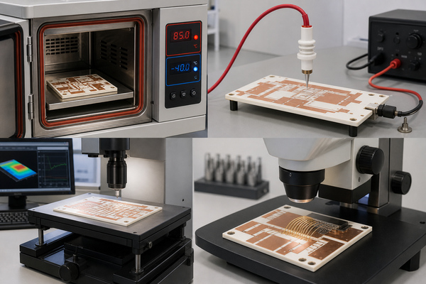
| Risk | Where it appears | Useful validation |
|---|---|---|
| Ceramic cracking | Large substrates, unbalanced copper, mounting stress or rapid thermal change | Visual and acoustic inspection, thermal shock, flatness and fixture review |
| Copper or metallization separation | High temperature swing and weak interface | Peel or adhesion testing before and after cycling |
| Solder or sinter fatigue | LED pads, die attach and substrate-to-baseplate joints | Thermal cycling, power cycling and cross-section analysis |
| Electrical insulation failure | IGBT, inverter and high-voltage converter modules | Hipot, insulation resistance and partial-discharge testing under defined conditions |
| Wire-bond degradation | Bare-die LED and power modules | Bond pull or shear testing before and after aging |
| Excess thermal resistance | Voids, poor TIM contact, wrong substrate grade or uneven mounting | Thermal transient measurement and correlation with the thermal model |
The acceptance criteria should be agreed before testing. "No visible damage" is not enough if thermal resistance, bond strength or partial-discharge inception voltage has moved outside the design margin.
When Is a Ceramic PCB Unnecessary?
A ceramic PCB is unnecessary when a less expensive construction meets all thermal, electrical and reliability limits. Low-power control electronics usually belong on FR4. Large LED boards with moderate heat flux may be well served by an aluminum MCPCB. A copper-core or insulated metal substrate may also be appropriate when heat spreading matters but high-voltage isolation, bare-die attachment or severe thermal cycling does not justify ceramic.
Do not select AlN simply because its thermal conductivity is high. If the dominant resistance is in the LED package, die attach, TIM or heat sink, changing the ceramic may produce little system benefit. Likewise, a power module with poor copper geometry or excessive solder voiding will not be rescued by a higher-conductivity substrate.
What Should Be Confirmed Before Prototyping?
A ceramic PCB prototype should test the intended construction, not a simplified board that removes the main risk. Before fabrication, confirm:
- ceramic material, grade, thickness and required thermal-conductivity value;
- metallization process, copper thickness and copper symmetry on both sides;
- final circuit artwork, line and gap, edge clearance, holes, cavities and singulation method;
- surface finish and whether the pads will be soldered, sintered or wire bonded;
- working voltage, isolation test, partial-discharge requirement and grounding arrangement;
- loss map, maximum operating temperature, cooling interface and mounting pressure;
- flatness, bow, dimensional tolerance and critical pad coplanarity;
- prototype quantity and the exact thermal, electrical and mechanical tests to be repeated on production units.
BSTCeramicPCB can review these inputs against the selected ceramic and metallization route before the prototype is released. The most useful early discussion is a list of critical limits and test methods, not a generic request for the "best ceramic PCB."
FAQ
1. What are ceramic PCBs used for?
Ceramic PCBs are used in high-power LEDs, IGBT and MOSFET modules, inverters, motor drives, power converters, laser modules, RF circuits, sensors and high-temperature hybrid electronics. They are most useful when heat transfer, electrical isolation and dimensional stability are required in the same substrate.
2. Which ceramic PCB is best for high-power LEDs?
Alumina DPC is a practical starting point for many LED modules. AlN DPC is preferred when thermal analysis shows that alumina is the limiting resistance or when heat is concentrated in a very small area. The correct choice also depends on die attach, copper pattern, TIM and heat-sink performance.
3. Why are ceramic substrates used in IGBT modules?
The substrate routes current, supports semiconductor dies, conducts heat to the cooler and electrically isolates the high-voltage circuit from the baseplate. DBC and AMB constructions provide copper conductors on an insulating ceramic layer for these combined functions.
4. Is DBC or AMB better for IGBT modules?
DBC is suitable for many established industrial and power-module designs. AMB on Si3N4 is often selected when mechanical strength and power-cycling reliability are more demanding. The decision should follow the module lifetime target, copper geometry and thermal-mechanical analysis.
5. Is AlN always better than alumina?
No. AlN has much higher thermal conductivity, but alumina is less expensive and may already meet the temperature target. AlN is justified only when lowering substrate thermal resistance provides a meaningful system-level benefit.
6. Can a ceramic PCB replace an MCPCB?
Yes, but replacement is not automatically necessary. Ceramic provides a more direct electrically insulating heat path and supports specialized die-attach and metallization structures. MCPCB remains appropriate for many moderate-power LED and power-control assemblies.
7. What causes ceramic PCB cracking?
Common causes include mechanical impact, excessive mounting force, unbalanced copper, sharp copper corners, large substrate dimensions, poor support, thermal shock and CTE mismatch within the assembly.
8. How is ceramic PCB thermal performance verified?
Use a thermal model supported by prototype measurements. Thermal transient testing, thermocouples at defined reference points and infrared imaging can help identify the resistance of the substrate, joints and cooling interface.
9. What surface finish is used for wire bonding?
The finish depends on wire material, bond process and reliability requirement. Nickel/gold systems and other bondable finishes may be used, but finish thickness, nickel condition, surface cleanliness and bond-pull acceptance criteria must be specified with the assembly process.
10. Are ceramic PCBs electrically conductive?
The ceramic substrate is electrically insulating. Copper, silver, gold or other metallization forms the conductive circuit on the ceramic surface or through designed vias.
Conclusion
Ceramic PCB applications in LEDs, IGBT modules and power electronics succeed when the substrate is selected as part of the complete thermal, electrical and mechanical stack. Alumina, AlN and Si3N4 solve different problems; DPC, DBC, AMB and thick film provide different conductor structures. Define the load, isolation and lifetime target first, then confirm the construction through representative prototypes and tests. For a project-specific review, contact BSTCeramicPCB at sales@bstceramicpcb.com.
 Products
 About us
 Contact us



