






















































 HOME


-

Ceramic PCB for Humanoid Robot joint actuators
2026 04,07 -
LTCC PCB Surprises: What Most People Miss
2025 12,09 -
Step-by-Step Guide to DPC PCB Design for Sensor Systems
2025 12,03 -
Ceramic PCBs Essential Benefits and Applications
2025 12,01 -
How Al2O3 DPC Ceramic Substrate PCB Enhances Heat Dissipation in Modern Electronics?
2025 11,28 -
How to Choose Between Ceramic, FR4, and Metal Core PCBs
2025 11,27 -
DPC Ceramic PCB Materials: Surprising Science Inside
2025 11,26 -
Wire bondable 2-layer Alumina substrates PCB | Bstceramic PCB
2025 09,22 -
Silicon Nitride Substrate, Silicon Nitride Ceramic Substrate Formula
2025 05,08 -
What is thick film ceramic PCB?
2023 08,02
Which Ceramic PCB Surface Finish Fits Your Assembly?
Published:
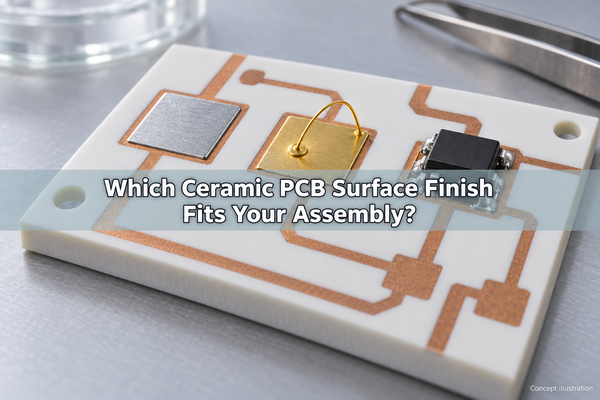
Choose a ceramic PCB surface finish for the connection it must make, not for its color. Solder-only copper pads may use OSP, immersion silver, immersion tin, or ENIG when the fabrication process supports them. Soldering combined with wire bonding often justifies evaluating ENEPIG or a qualified gold stack. Sliding contacts require a separate wear specification. The conductor beneath the finish and every assembly step must remain compatible with that choice.
Identify the Conductor Before Choosing Its Finish
The finish normally protects or modifies an exposed conductor; it is not a coating that makes bare ceramic solderable. A ceramic PCB substrate may carry plated copper, bonded copper, a thin-film metal stack, or a fired thick-film conductor. Those constructions do not accept an identical finishing process by default.
On copper circuits, ENIG and ENEPIG add layers above copper. In thick-film circuitry, a fired gold or silver-palladium conductor can itself provide the functional exposed surface. Our AgPd thick-film ceramic circuits illustrate this distinction: the conductor system must be specified before assuming that a conventional copper-board finish can be substituted.
Record the base conductor, any adhesion layer, existing barrier layer, and exposed pad locations. A purchase note that says only "gold finish" leaves the electrically and mechanically important layers undefined.
Shortlist Finishes by Connection Type
A useful PCB surface finishes comparison starts with the required joint or contact. The options below are candidates for engineering review, not interchangeable approvals for every ceramic process.
| Connection requirement | Candidate finish | Main selection boundary |
|---|---|---|
| Solder-only copper pads, controlled storage | OSP | Protects copper before assembly; handling and repeated heat exposure need control |
| Flat solder pads without a nickel barrier | Immersion silver | Check sulfur exposure, packaging, and corrosion requirements |
| Solderable copper pads using a tin process | Immersion tin | Confirm aging, whisker risk controls, and the available assembly window |
| Fine-pitch solder assembly | ENIG | Qualify nickel integrity and solder-joint reliability |
| Soldering plus wire bonding | ENEPIG | Verify the actual wire, bonding process, and thermal history |
| Dedicated gold-wire bonding surface | Qualified soft-gold stack | Define purity, underlying metals, thickness, and bond test criteria |
| Repeated wiping or mating | Qualified hard-gold contact system | Specify wear cycles and contact resistance; do not treat it as a general bond pad |
| Nickel-restricted RF or magnetic-sensitive circuit | Qualified nickel-free stack, such as an appropriate Pd/Au system | Confirm availability and electrical, soldering, or bonding performance on the actual circuit |
The least complex finish that passes the required tests is usually a better starting point than specifying a premium finish across every exposed surface.
Decide Whether a Non-Gold Finish Is Sufficient
Gold is unnecessary when the assembly only needs a solderable copper interface and a less expensive finish meets the storage and reliability requirements. OSP, immersion silver, and immersion tin deserve consideration before gold is added solely as a quality signal.
OSP is attractive for controlled solder-only production, but its condition after handling and multiple thermal excursions matters. Immersion silver avoids a nickel barrier but requires packaging and environmental controls appropriate to tarnishing and sulfur exposure. Immersion tin requires attention to copper-tin intermetallic growth during aging and a documented approach to tin-whisker risk where that risk matters.
Do not copy an FR4 supplier's menu directly onto a ceramic drawing. Confirm that the ceramic circuit manufacturer supports the chosen chemistry on the conductor, mask or glaze, feature size, and panel construction being ordered. Availability on one ceramic product does not establish availability on every other product.
Build a Compatibility Map for the Assembly Sequence
A finish must survive the steps before its final connection is made. List soldering, cleaning, die attachment, wire bonding, and encapsulation in their actual order, then identify which exposed pads remain unfinished at each stage.
For example, an LED substrate may have soldered external terminals and bond pads that remain exposed through an earlier heat cycle. Qualifying a fresh bond pad alone would miss that thermal history. Our alumina DPC LED substrates include an ENEPIG-finished construction; the combination makes mixed joining requirements relevant, but each assembly still needs its own qualification.
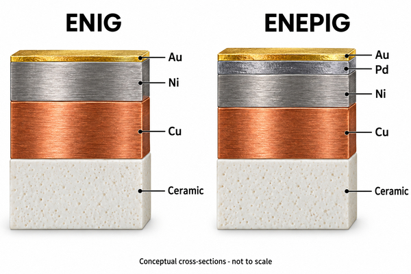
ENIG has nickel followed by immersion gold. ENEPIG inserts palladium between those layers, changing the interface exposed during bonding and soldering. That additional layer can support mixed assembly needs; it does not remove the need to control plating chemistry, cleanliness, and bondability. Conventional ENIG should not be accepted for gold-wire bonding merely because it looks gold.
For a nickel-restricted design, identify the reason: RF loss, magnetic response, or another system constraint. Evaluate the complete conductor stack at the operating frequency or magnetic condition. Nickel-phosphorus composition and thermal history matter, so neither "all nickel finishes are equivalent" nor "gold guarantees low loss" is an adequate specification.
Separate Bond Pads From Wear Contacts
Bonding and repeated mechanical contact require different surface behavior. Soft gold is used in qualified bonding systems, while hard gold is selected for wear resistance. Hardening additives and the chosen underplate can make a contact finish unsuitable for a bonding process.
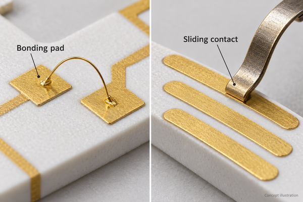
Define the interface on the drawing: wire material and bonding method for bond pads; mating material, contact force, wiping distance, and cycle requirement for contacts. Do not specify the same gold thickness simply because both areas share the same color. Gold entering a small solder joint also requires review of alloy composition and joint volume rather than an assumption that thicker is always better.
Compare One Finish With Selective Finishing
One qualified finish across all required pads simplifies ordering and inspection. Selective finishing becomes useful when no single stack satisfies soldering, bonding, and contact-wear requirements without unnecessary cost or compromise.
Mark finish regions explicitly and keep the boundaries away from critical joint footprints where feasible. Ask about masking accuracy, plating access, coverage around pad edges, and whether narrow gaps remain manufacturable after deposition. Selective electrolytic plating may require temporary electrical connections; these must be reconciled with the final circuit pattern.
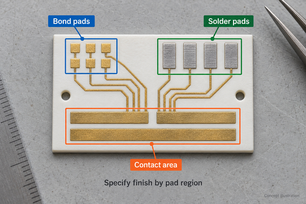
Evaluate selective processing using the same finished geometry and test scope as the uniform-finish alternative. Selective processing can reduce precious-metal area while adding masking, handling, and inspection work. It is not automatically cheaper than a uniform finish, especially for a small prototype batch.
Specify PCB Surface Finish Thickness Layer by Layer
PCB surface finish thickness must identify the individual metal, its allowable range, and the measurement location. Total stack thickness does not tell an assembler how much gold can dissolve into solder or whether a barrier layer meets its requirement.
Use one unit consistently: 1 microinch equals 0.0254 micrometers. A note such as "3 microinches gold" corresponds to 0.0762 micrometers of gold; it does not define the nickel or palladium beneath it. Treat this as a unit conversion, not a recommended thickness for every joint.
Specify the applicable finish standard and revision where relevant, together with product-specific requirements. Include minimum and maximum thicknesses, sampling locations, and the agreed measurement method. X-ray fluorescence can measure appropriate coating stacks when calibrated for those materials and geometry; a small or irregular pad may require a different coupon or verification approach.
On our DBC ceramic circuits for automotive components, thick copper and an ENEPIG finish perform separate jobs. Copper thickness is not a substitute for a finish-layer specification, and a large power pad should be included in the inspection plan rather than inferred from a small test point alone.
Include Storage and Handling in the Selection
Shelf life is conditional on the finish chemistry, packaging, atmosphere, and handling history. Do not assign every gold finish twelve months or every silver finish six months without the supplier's applicable conditions.
Specify sealed packaging, allowed storage conditions, maximum time after opening, and whether boards will undergo incoming inspection before resealing. Avoid touching bond or solder pads. For silver surfaces, consider sulfur-bearing packaging and the expected operating environment. For OSP, confirm permitted cleaning and baking practices rather than applying a generic bake that may degrade the protective layer.
If assemblies wait between reflow and bonding, include that queue time in prototype validation. Surface cleanliness immediately after fabrication is not proof of cleanliness at the bonding station several weeks later.
Match Acceptance Tests to the Intended Interface
Visual appearance and a thickness report are not enough to prove functional suitability. Use tests that challenge the failure mode of the actual connection.
| Intended function | Verification to agree | What the result should establish |
|---|---|---|
| Solder attachment | Solderability testing using the intended alloy and representative aging; joint inspection | Wetting and acceptable joints after the expected process history |
| Wire bonding | Bond pull and, where applicable, ball shear with failure-mode recording | Bond integrity, not just a peak force on fresh samples |
| Sliding contact | Contact resistance before and after representative cycling | Stable electrical contact under the specified mechanical conditions |
| Coating conformity | Calibrated thickness measurement and agreed sampling | Each specified layer is within its limits |
| Harsh-environment use | Relevant corrosion or humidity exposure followed by functional checks | The selected finish survives the actual environmental risk |
Investigate brittle joints, corrosion, or pad lifting rather than trying to fix them by adding more gold. A palladium barrier can reduce nickel attack during immersion-gold processing, but describing ENEPIG as immune to every plating or assembly defect is not justified.
Control Finish Substitutions Before Production
Treat a finish change as an engineering change, not a cosmetic purchasing substitution. Replacing ENIG with ENEPIG changes the stack; replacing a gold finish with silver changes storage and environmental considerations; changing the thick-film conductor can alter the interface even when the surface looks similar.
Approve the revised stack, pad regions, assembly sequence, packaging, and acceptance criteria together. Run a representative prototype through the complete planned process before releasing volume production. Keep the approved drawing revision and the finish designation aligned with purchase orders and inspection records.
A suitable ceramic PCB surface finish is one that meets the connection and handling requirements without unnecessary processing. At BSTCeramicPCB, we provide DPC, DBC, and thick-film ceramic circuit options. Send your conductor construction, pad-region drawing, assembly sequence, and required tests to sales@bstceramicpcb.com so we can review the finish requirements for a quotation.
 Products
 About us
 Contact us



