






















































 HOME


-

Ceramic PCB for Humanoid Robot joint actuators
2026 04,07 -
LTCC PCB Surprises: What Most People Miss
2025 12,09 -
Step-by-Step Guide to DPC PCB Design for Sensor Systems
2025 12,03 -
Ceramic PCBs Essential Benefits and Applications
2025 12,01 -
How Al2O3 DPC Ceramic Substrate PCB Enhances Heat Dissipation in Modern Electronics?
2025 11,28 -
How to Choose Between Ceramic, FR4, and Metal Core PCBs
2025 11,27 -
DPC Ceramic PCB Materials: Surprising Science Inside
2025 11,26 -
Wire bondable 2-layer Alumina substrates PCB | Bstceramic PCB
2025 09,22 -
Silicon Nitride Substrate, Silicon Nitride Ceramic Substrate Formula
2025 05,08 -
What is thick film ceramic PCB?
2023 08,02
How Can You Measure and Control Ceramic PCB Warpage?
Published:
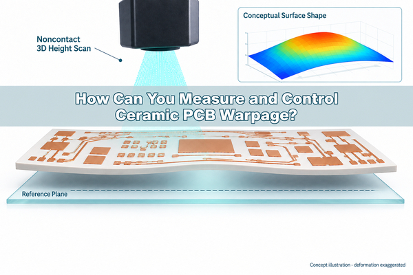
Ceramic PCB warpage is the out-of-plane deformation of a ceramic circuit substrate. It can change solder-joint gaps, die-attach thickness and contact with a heat spreader even when the board outline and thickness meet their drawings. Control starts with specifying which surface must be flat, over what area, at what temperature and under what support condition. A room-temperature measurement alone cannot establish how the substrate will behave during assembly.
Distinguish Bow, Twist and Local Flatness
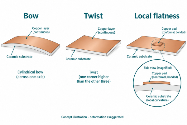
Bow is an overall curved shape, while twist describes a change in the relative plane of the corners. Local flatness concerns a defined region, such as the footprint beneath a power die or the backside area contacting a cooler. A substrate can have modest overall bow but still have an unacceptable local mounting surface.
Do not combine copper thickness steps with substrate deformation. A height scan crossing an etched copper edge records a designed step as well as any curvature. Identify whether the inspected surface is exposed ceramic, a continuous copper region or the tops of selected attachment pads before calculating a result.
Why Do Copper and Ceramic Bend Together?
Copper and ceramic expand differently during heating and contract differently during cooling. Once bonded together, they constrain each other. An asymmetric combination of layer thickness, stiffness and residual stress can bend the substrate. The final shape also depends on processing history; a room-temperature expansion-coefficient comparison does not predict warpage by itself.
For our DBC ceramic boards for automotive components, copper distribution on both faces is an important design input. Equal nominal copper thickness does not guarantee balance after etching: one face may retain a broad metal area while the other becomes isolated tracks and pads.
DPC structures introduce another variable: the residual stress of deposited metal. Our alumina DPC ceramic substrates for LED assembly use patterned copper, so the review should consider both the deposited layer and the remaining pattern. A thin conductor is not proof that the finished substrate will be flat.
Find the Process Step That Changes the Shape
Compare the same identified parts at successive stages. A final inspection shows the defect, but stage-by-stage records help distinguish incoming ceramic shape from metallization, singulation or assembly effects.
| First observed change | What to compare | What the comparison can establish |
|---|---|---|
| Incoming bare ceramic | Material lot, dimensions, thickness and initial surface map | Whether the starting substrate already contains the deviation |
| After metallization or firing | Before/after maps, metal thickness and process history | Whether the change appears during metal deposition, bonding or firing |
| After patterning | Remaining copper regions on both faces and panel position | Whether removal of metal changes the stress balance |
| After singulation | Panel and individual-part maps with equivalent references | Whether releasing panel constraints changes the shape |
| During heating | Shape at specified temperatures and dwell times | Whether deformation is temperature-dependent |
| After component attachment or mounting | Free-state and assembled measurements | Whether joints, adhesive cure or mechanical constraint introduce distortion |
Our thick-film alumina circuits for automotive sensing use fired conductor structures. For this type of circuit, comparisons before and after firing are more informative than assuming every shape change comes from thick copper. Where several firing steps are used, retain the sequence with the measurements.
Measure the Same Surface Under the Same Conditions
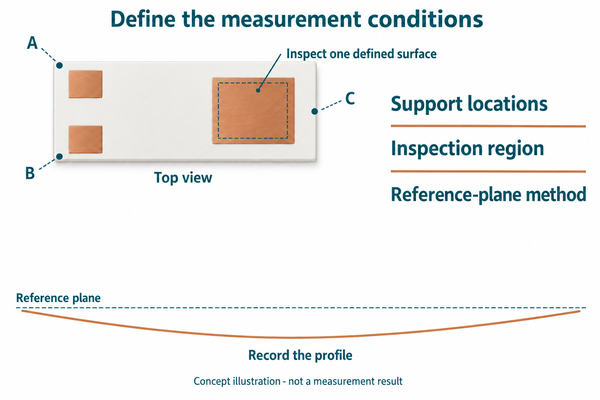
A repeatable measurement requires a defined reference, support arrangement and orientation. Clean loose particles from the support and inspected surface using an approved method. Record the part ID, inspected face, temperature, support locations and whether the sample is free or constrained. Do not press a brittle ceramic substrate flat to obtain a smaller reading.
A calibrated optical height measurement can characterize a full surface without probe loading. Reflective copper and exposed ceramic may produce different optical responses, so validate the instrument settings on the actual surface combination. A contact method can also be suitable, but probe force and support-induced movement must be evaluated.
Choose the calculation before comparing suppliers. Maximum departure from a specified reference plane, peak-to-valley height after plane fitting, corner lift and geometric flatness are not interchangeable outputs. Record the fitting method, masked areas, sampling density and uncertainty. A visually convincing color map without those settings is not a complete inspection record.
Check Hot Warpage as Well as Room-Temperature Shape
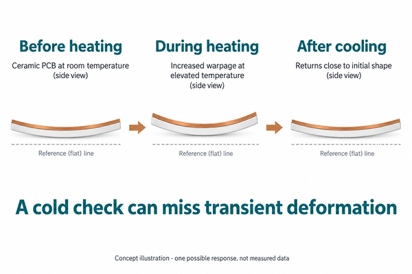
Measure at temperatures that correspond to the actual process or operating condition. A substrate can meet its cold requirement and change shape during soldering, sintering or adhesive cure. It may also return close to its original shape after cooling, concealing the maximum gap experienced while a joint was forming.
Use a representative thermal cycle and record heating rate, dwell, cooling conditions and fixture configuration. Compare incoming, heated and cooled states on the same part where practical. Do not assume that the worst deformation occurs at the highest temperature, or that a hot measurement on a bare substrate represents a populated module.
If the finished assembly is clamped to a cooler, distinguish free-state substrate behavior from the constrained assembly response. Both can matter, but they answer different questions. A clamp can reduce visible displacement while increasing local stress.
Translate Flatness Into an Assembly Gap Budget
Start from the attachment interface, not a generic percentage. Determine how much variation the solder, sintered layer, adhesive or thermal-interface material can accommodate while maintaining the specified bond-line thickness and contact. Include the mating component, cooler flatness and positioning tolerances in the same assessment.
| Interface | Consequence of excessive shape variation | Relevant region to evaluate |
|---|---|---|
| Large power die | Uneven attachment thickness, incomplete contact or stress concentration | Die footprint and surrounding attachment area |
| Surface-mount component | Unequal terminal gaps during joint formation | Actual pad group at assembly temperature |
| Substrate-to-baseplate attachment | Bond-line variation and uneven load transfer | Full bonded area, including edge regions |
| Clamped thermal interface | Uneven contact pressure and interface thickness | Cooler contact area under the specified mounting condition |
Span matters. In an idealized, shallow circular bow, center sag is approximately curvature multiplied by span squared, divided by eight. At an assumed curvature of 0.1 per meter, a 20 mm span gives about 5 micrometers of sag; a 40 mm span gives about 20 micrometers. These are geometric examples, not acceptance limits. They explain why enlarging a substrate can increase the gap even without changing its curvature.
Set a Ceramic PCB Warpage Specification That Can Be Verified
A useful PCB warpage spec identifies the measured quantity and the acceptance conditions together. A drawing note that says only "flatness 0.1%" leaves the denominator, inspected area and support condition unresolved. State the required result in an agreed unit, and define any percentage calculation explicitly.
IPC-TM-650 2.4.22 describes bow and twist measurement for bare rigid printed boards and panels; it is not a universal ceramic-substrate acceptance limit or an assembly qualification. Bow and twist calculations are method-specific. Do not apply a familiar FR-4 percentage or an unspecified diagonal formula to every ceramic circuit.
Include these items in the drawing or inspection agreement:
- Inspected face and region, including any excluded holes, copper steps or edge zones.
- Free-state or constrained measurement, support positions and orientation.
- Temperature, thermal history and stabilization condition.
- Reference-plane or flatness evaluation method and the reported quantity.
- Maximum allowable deviation, measurement uncertainty and sampling plan.
- Required stages: incoming, after metallization, after assembly or after thermal cycling.
Use a separate local requirement when a critical attachment pad needs tighter control than the whole board. This avoids paying for an unnecessarily tight global tolerance while leaving the functional region poorly defined.
Reduce Bending With Copper Layout and Stackup Choices
Review metal coverage by region on opposite faces, not only the total copper percentage. Two layouts can have the same overall coverage but very different distributions around a large die pad, an isolation slot or an edge. Consider copper thickness, ceramic thickness, panel arrangement and the intended singulation sequence together.
Where electrical and thermal requirements permit, balancing metal regions or changing large uninterrupted areas may reduce asymmetry. Dummy metal must still satisfy clearance, isolation, parasitic-capacitance and thermal-path requirements. Adding copper solely to improve a coverage statistic can create a different design problem.
Increasing ceramic thickness can increase bending stiffness, but it also changes the thermal path and package geometry. Reducing copper thickness changes current capacity and heat spreading. Evaluate these as coupled changes using the actual material stackup; there is no universally best copper-to-ceramic thickness ratio.
Handle and Mount a Warped Substrate Without Forcing It Flat
Do not treat a warped ceramic PCB board like a flexible laminate. Unqualified bending, pressing or screw tightening can produce cracks or damage the metal-ceramic interface. If a part is outside its agreed limit, quarantine it and compare the measured profile with the approved drawing before attempting rework.
Support the substrate near functional mounting regions and avoid concentrated loads on unsupported ceramic. Define the assembly torque, tightening sequence and permitted support materials as part of the mounting design. A thermal pad should be selected for the actual gap and pressure range, not used to conceal an unknown deformation.
Heating under a weight is not a general repair method. Any proposed flattening or stress-relief operation needs an approved process and subsequent dimensional, electrical and relevant reliability verification. Replacing an out-of-spec part may be safer and more economical than introducing an unqualified recovery step.
Validate the First Article Before Releasing the Design
Use the ceramic PCB prototype to establish the relationship between measured shape and assembly performance. Inspect multiple parts and relevant panel positions, retain the raw maps, and repeat the critical measurements after the intended attachment and thermal cycle. A single passing part does not establish lot-to-lot capability.
Release the design only when the specified measurement is repeatable and the interface remains acceptable under its working conditions. Keep the approved stackup, copper pattern, inspection settings and thermal process connected to the results. A later change in metal coverage or ceramic thickness should trigger a review of that evidence.
Controlling ceramic PCB warpage means connecting the surface requirement to the manufacturing stage and assembly interface. At BSTCeramicPCB, we offer DPC, DBC and thick-film ceramic circuits. Send the two-sided layout, stackup, critical attachment areas and proposed inspection conditions to sales@bstceramicpcb.com so we can review the circuit requirements before quotation; any requested flatness limit needs project-specific confirmation.
 Products
 About us
 Contact us



