






















































 HOME
HOME


-

Ceramic PCB for Humanoid Robot joint actuators
2026 04,07 -
LTCC PCB Surprises: What Most People Miss
2025 12,09 -
Step-by-Step Guide to DPC PCB Design for Sensor Systems
2025 12,03 -
Ceramic PCBs Essential Benefits and Applications
2025 12,01 -
How Al2O3 DPC Ceramic Substrate PCB Enhances Heat Dissipation in Modern Electronics?
2025 11,28 -
How to Choose Between Ceramic, FR4, and Metal Core PCBs
2025 11,27 -
DPC Ceramic PCB Materials: Surprising Science Inside
2025 11,26 -
Wire bondable 2-layer Alumina substrates PCB | Bstceramic PCB
2025 09,22 -
Silicon Nitride Substrate, Silicon Nitride Ceramic Substrate Formula
2025 05,08 -
What is thick film ceramic PCB?
2023 08,02
Ceramic Substrate for EV Inverter: DBC, AlN and Supplier Selection
Published:
Ceramic substrate for EV inverter applications must carry high current, isolate high voltage and move heat from IGBT or SiC devices into the cooling structure. The right substrate is not chosen by thermal conductivity alone; it also depends on copper thickness, ceramic material, bonding process, insulation distance, thermal cycling, partial discharge risk and the supplier’s ability to control copper-ceramic adhesion.
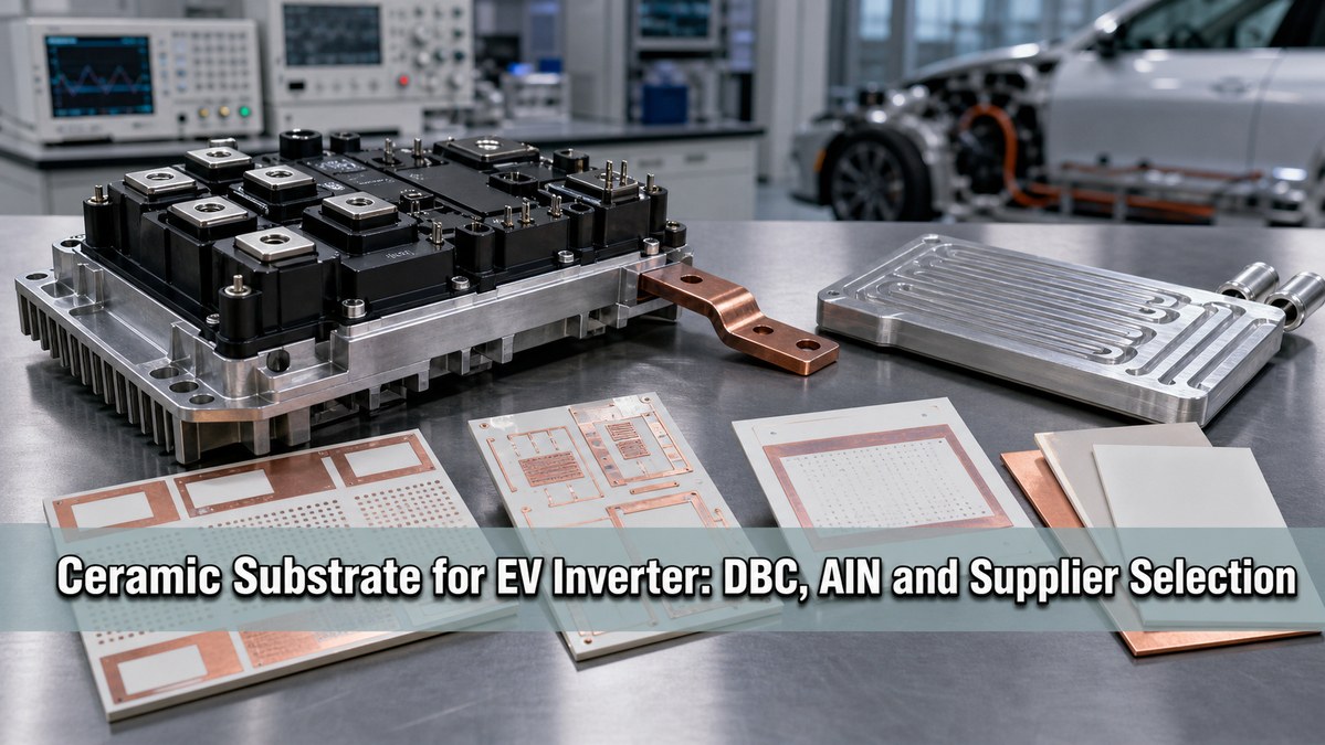
In an EV traction inverter, the substrate sits inside the power module between the semiconductor dies and the heat removal path. A weak choice can increase junction temperature, crack solder or sintered layers, lift copper edges, reduce insulation margin or fail after repeated power cycling. A strong choice starts from the inverter platform, semiconductor type, current density, cooling method and reliability target.
What Is a Ceramic Substrate for EV Inverter?
A ceramic substrate for EV inverter is an electrically insulating, thermally conductive base used in power modules to support IGBT, SiC MOSFET or diode chips. It normally combines a ceramic layer with copper metallization so the module can route current while transferring heat to a baseplate, cooler or double-sided cooling stack.
The most common structures are DBC, DCB, AMB and, in some lower-current or fine-line cases, DPC. In EV inverter modules, the substrate must survive wider temperature swings and stronger mechanical stress than ordinary control electronics, so the material and copper bonding route should be reviewed together.
Why Do EV Inverters Need Ceramic Substrates Instead of Standard PCB Materials?
EV inverters need ceramic substrates because standard PCB laminates cannot provide the same combination of high-voltage insulation, heat transfer, copper current capacity and thermal cycling stability. FR4 or high-Tg PCB materials are suitable for gate drivers, control boards and low-power circuits, but the main power stage needs a substrate designed for semiconductor packaging.
A ceramic power substrate separates high-voltage copper patterns from the cooler while keeping thermal resistance low. This is critical in compact automotive modules where heat source density, switching speed and vibration all increase reliability pressure.
Which Ceramic Substrate Technologies Are Used in EV Inverter Modules?
DBC and AMB are the main ceramic-copper substrate technologies for EV inverter power modules. DBC bonds copper directly to ceramic through a controlled high-temperature oxidation reaction, while AMB uses active brazing alloy to bond copper to ceramic, especially for materials that need stronger mechanical reliability.
| Technology | Best Fit | Main Engineering Note |
|---|---|---|
| DBC / DCB | Alumina or AlN substrates for established power modules | Good thermal path and high current capacity; copper pattern limits are coarser than thin-film routes |
| AMB | High-reliability Si3N4 or AlN power substrates | Often selected when thermal cycling and mechanical strength are more demanding |
| DPC | Fine-line ceramic PCB, sensors and compact modules | Better line definition, but copper thickness is usually lower than heavy DBC/AMB power substrates |
| Thick film | Hybrid circuits, sensors and resistor networks | Useful for functional ceramic circuits, but not the default for high-current traction inverter substrates |
How Should You Choose Between Al2O3, AlN and Si3N4?
Choose Al2O3 when cost, availability and mature processing matter more than maximum heat spreading. Choose AlN when thermal conductivity and closer CTE alignment to semiconductor devices are more important. Choose Si3N4 when mechanical strength, fracture toughness and power cycling reliability are the dominant risks.
For EV inverter projects, AlN DBC may be attractive for thermal performance, while Si3N4 AMB is often reviewed when the module faces aggressive thermal cycling or high mechanical stress. Alumina DBC can still be practical for lower power density or cost-sensitive modules, but it needs careful thermal design and validation.
When Is DBC Ceramic Substrate Suitable for EV Inverter Design?
DBC ceramic substrate is suitable when the module needs thick copper, good insulation and a proven ceramic-copper structure. It is commonly used with alumina or AlN, and it can support high-current power paths better than thin metallization processes.
The limits are copper pattern resolution, edge stress and ceramic cracking risk under severe cycling. If the design uses large copper islands, sharp copper corners, thick copper or strong thermal gradients, the layout should include rounded corners, balanced copper and enough edge clearance. Related process context is covered in Fabrication Processes Of DCB Ceramic Substrate PCB.
When Should AlN DBC Substrate Be Considered?
AlN DBC substrate should be considered when the inverter power density is high and the thermal path from die to cooler must be improved without moving to a different module architecture. AlN offers much higher thermal conductivity than alumina and can help reduce thermal resistance in compact modules.
AlN is more expensive and more sensitive to process control than standard alumina. Before specifying it, confirm the target copper thickness, surface finish, ceramic thickness, dielectric requirement, thermal cycling condition and whether the supplier has experience with AlN metallization and inspection. A related material reference is What is Aluminum Nitride Ceramic Substrate?.
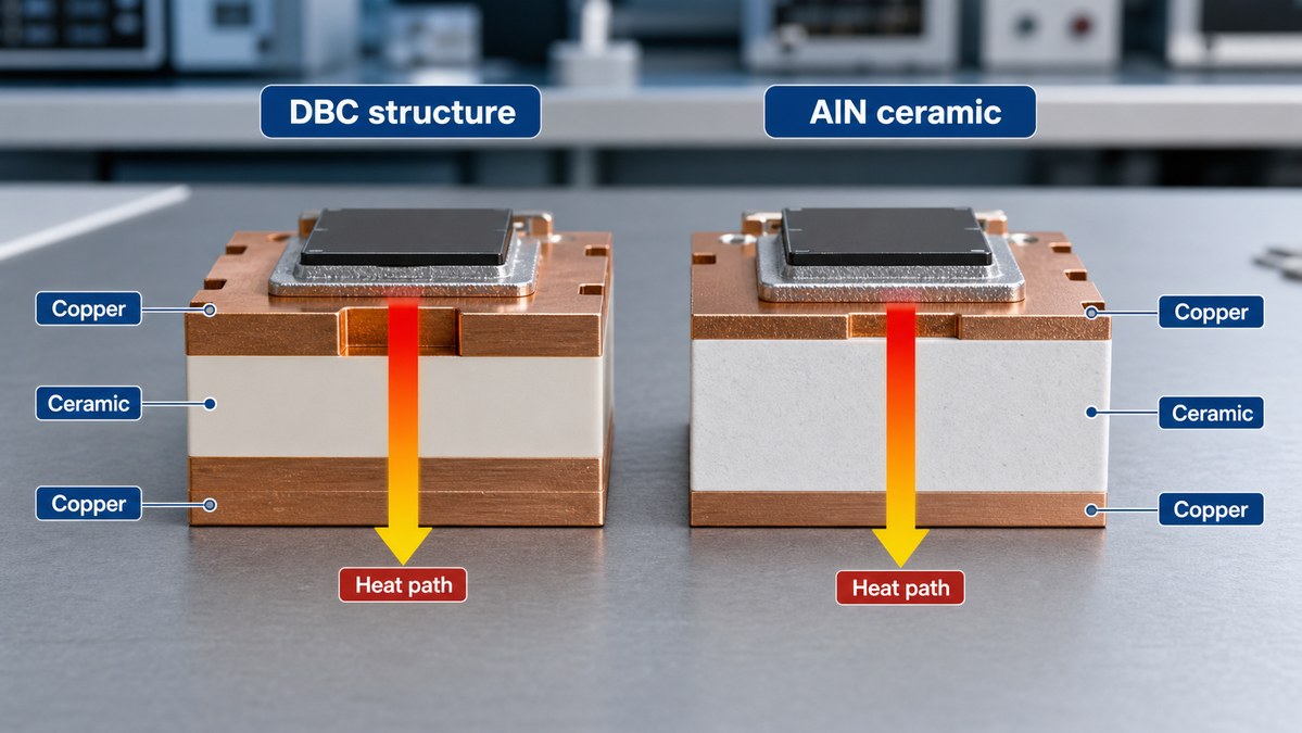
How Do Copper Thickness and Ceramic Thickness Affect Performance?
Copper thickness affects current capacity, spreading resistance, etching limits and mechanical stress. Thicker copper can carry more current and spread heat better, but it also increases force on the ceramic during heating and cooling. Ceramic thickness affects insulation strength and thermal resistance; a thicker ceramic improves voltage margin but raises the heat path resistance.
For EV inverter substrates, the copper and ceramic thickness should be reviewed as a pair, not as separate line items. A design with thick copper on a thin ceramic may need special attention to copper balance, corner radius and stress relief. A design with conservative ceramic thickness may pass insulation checks but lose thermal performance.
What Reliability Risks Should Be Checked Early?
The main reliability risks are copper delamination, ceramic cracking, solder or sinter fatigue, insulation degradation, partial discharge, copper edge lifting and metallization corrosion. These risks often appear after repeated temperature swing, high current pulse loading or humidity-bias exposure.
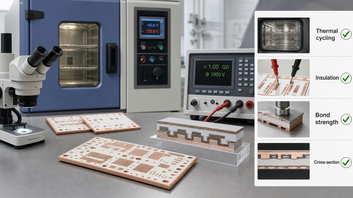
Early validation should include thermal cycling, power cycling assumptions, dielectric withstand, partial discharge where relevant, copper peel or bond strength, dimensional inspection and cross-section review. If the module uses SiC devices, switching speed and local heat density should be included in the substrate review rather than treated only as electrical design topics.
How Does the Ceramic Substrate Manufacturing Process Affect EV Inverter Quality?
The manufacturing process controls the copper-ceramic interface, copper pattern accuracy, plating quality, insulation clearance and final substrate flatness. For DBC, process control around copper oxidation, bonding temperature, atmosphere, etching and plating is essential. For AMB, braze alloy control, voiding, wetting and post-braze inspection become central.
Typical process steps include ceramic preparation, copper bonding or brazing, photoresist imaging, copper etching, surface treatment, singulation, cleaning and inspection. The exact sequence depends on DBC, AMB, DPC or thick-film technology. For a DBC introduction, see What is DBC Ceramic PCB?.
What Design Data Should Engineers Prepare Before RFQ?
An RFQ should include the electrical, thermal and mechanical assumptions needed to judge risk. A drawing that only states “ceramic substrate” is not enough for EV inverter work because the supplier must know current path, insulation distance, ceramic grade, copper thickness, thermal cycle and assembly method.
- Substrate technology: DBC, AMB, DPC or requested alternative
- Ceramic material: Al2O3, AlN, Si3N4 or specified supplier grade
- Copper: thickness, layout, minimum line/space, corner radius and copper balance
- Electrical: bus voltage, isolation requirement, creepage/clearance and partial discharge target
- Thermal: heat source size, cooling method, operating temperature and cycling profile
- Assembly: die attach, soldering or sintering, wire bonding, surface finish and cleanliness needs
- Files: Gerber, DXF, stackup, material note, tolerance drawing and expected annual quantity
How Should You Evaluate a Ceramic Substrate Supplier?
Evaluate a ceramic substrate supplier by checking whether they can explain the material route, copper bonding method, inspection plan and design limits for your inverter platform. A supplier that only quotes price from a drawing may miss thermal cycling, copper stress or insulation risks.
BSTCeramicPCB can support ceramic PCB and ceramic substrate discussions across Al2O3, AlN, DBC/DCB, AMB, DPC and thick-film routes. The useful conversation should focus on manufacturability, prototype verification, copper-ceramic bonding quality, surface finish and test expectations rather than generic material claims. For direct inquiry, use Ceramic Substrate PCB Quote.
What Should Be Validated Before Prototype and Mass Production?
Before prototype release, validate the stackup, copper geometry, insulation distance, substrate outline, mounting interface and thermal model. Before mass production, validate process repeatability, incoming material control, copper bond strength, plating consistency, dimensional capability, cleaning and packaging.
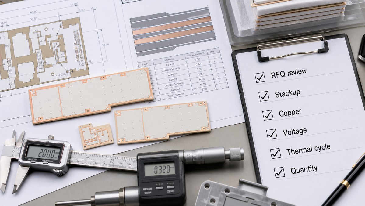
Prototype checks should answer whether the design can be made and assembled. Mass production checks should answer whether the same substrate can be made repeatedly with acceptable yield and reliability. Keep prototype changes traceable, especially copper pattern changes, ceramic thickness changes and surface finish changes.
How Can Ceramic Substrate Choices Reduce EV Inverter Failure Risk?
Ceramic substrate for EV inverter reliability improves when the material, copper pattern, cooling interface and validation plan are selected together. A substrate with high thermal conductivity can still fail if copper stress, ceramic toughness, voiding or insulation clearance is ignored.
The best practical approach is to define the module duty cycle, select a candidate ceramic technology, review copper and ceramic thickness, prototype the thermal and mechanical stack, then confirm reliability tests before scaling. This keeps the substrate choice tied to the real inverter environment rather than to a single material property.
FAQ
1. Is DBC ceramic substrate the same as DCB?
In many industry contexts, DBC and DCB both refer to direct bonded copper ceramic substrates. Naming varies by supplier, but the key point is copper bonded directly to ceramic without an organic adhesive layer.
2. Is AlN always better than alumina for EV inverter substrates?
No. AlN offers higher thermal conductivity, but alumina may still be suitable for lower power density or cost-sensitive designs. The decision should include heat flux, voltage, copper thickness, reliability target and budget.
3. Why is Si3N4 often discussed for automotive power modules?
Si3N4 is valued for mechanical strength and fracture toughness, which can help under demanding thermal cycling. It is often reviewed with AMB structures for high-reliability automotive power modules.
4. Can a ceramic substrate replace a standard PCB in an EV inverter?
It replaces the high-power module substrate, not the entire inverter electronics. Control circuits, gate drivers and sensing boards may still use conventional PCB technologies.
5. What is the most important information for a supplier quote?
The most important information is the substrate technology, ceramic material, copper thickness, insulation requirement, thermal cycle, surface finish, Gerber/DXF files and expected production quantity.
Conclusion
A ceramic substrate for EV inverter should be selected through the full power-module context: semiconductor type, thermal path, copper design, insulation margin, cycling reliability and manufacturing control. DBC, AlN DBC, AMB and other ceramic substrate routes all have valid use cases, but the right choice depends on the inverter platform and validation plan. For ceramic substrate PCB review, prototype discussion or supplier quotation, contact BSTCeramicPCB at sales@bstceramicpcb.com.
 Products
 About us
 Contact us



