






















































 HOME


-

Ceramic PCB for Humanoid Robot joint actuators
2026 04,07 -
LTCC PCB Surprises: What Most People Miss
2025 12,09 -
Step-by-Step Guide to DPC PCB Design for Sensor Systems
2025 12,03 -
Ceramic PCBs Essential Benefits and Applications
2025 12,01 -
How Al2O3 DPC Ceramic Substrate PCB Enhances Heat Dissipation in Modern Electronics?
2025 11,28 -
How to Choose Between Ceramic, FR4, and Metal Core PCBs
2025 11,27 -
DPC Ceramic PCB Materials: Surprising Science Inside
2025 11,26 -
Wire bondable 2-layer Alumina substrates PCB | Bstceramic PCB
2025 09,22 -
Silicon Nitride Substrate, Silicon Nitride Ceramic Substrate Formula
2025 05,08 -
What is thick film ceramic PCB?
2023 08,02
Ceramic Surface Roughness: Ra, Rz, Measurement and PCB Effects
Published:
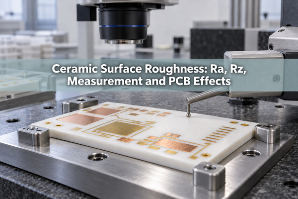
Ceramic surface roughness describes the small-scale peaks and valleys on a ceramic substrate after firing, grinding, lapping, or polishing. For PCB and electronic-package buyers, the number is useful only when it is tied to a parameter, unit, measurement method, surface condition, and downstream process. An Ra limit that works for thick-film paste may be unnecessarily costly for a power substrate, while a rough or defect-rich surface can interrupt fine thin-film conductors.
What Is Ceramic Surface Roughness?
The surface roughness of ceramic is its short-wavelength surface texture. It is not the same as flatness, bow, warpage, waviness, porosity, or isolated damage. A substrate can have a low Ra value and still be unsuitable because it is bowed, contains open pores, or has edge chips. It can also be flat overall but too rough for fine photolithography.
For purchasing and inspection, the surface must be identified precisely. “Polished side,” “circuit side,” and “both sides” are different requirements. The drawing should also state whether the value applies to bare ceramic, a metallized surface, or a finished bond pad.
What Do Ra, Rz and Sa Measure?
Ra, Rz, and Sa describe different features, so they should not be treated as interchangeable values.
| Parameter | What it represents | Practical use | Important limitation |
|---|---|---|---|
| Ra | Arithmetic mean of deviations along a filtered profile | Common drawing and supplier specification | Averaging can hide an isolated high peak or deep valley |
| Rz | Peak-to-valley height characteristic over defined sampling lengths | More sensitive to pronounced peaks and valleys | The exact definition and evaluation rules depend on the referenced standard |
| Sa | Arithmetic mean height over an areal, three-dimensional dataset | Useful for optical topography and non-directional surface assessment | Results depend on scan area, filtering, instrument settings, and data treatment |
A buyer asking for “Ra 0.1” without units, standard, cutoff, or measurement location has not created a complete acceptance criterion. The same surface can produce different values when the evaluation conditions change.
Why Can Two Roughness Measurements Disagree?
Disagreement is often caused by the measurement setup rather than a material change. The main variables are:
- stylus tip radius and measuring force;
- cutoff, filter, sampling length, and evaluation length;
- trace direction relative to grinding or lapping marks;
- optical objective, scan area, thresholding, and missing-data treatment;
- the selected location and whether pores or scratches were included;
- the standard and parameter definition used by the instrument.
This is why a supplier certificate and an incoming-inspection report may conflict even when both instruments are calibrated. Before rejecting a lot, compare the parameter, unit, standard, filter, measurement direction, evaluation length, and inspection zone.
How Is Ceramic Surface Roughness Measured?
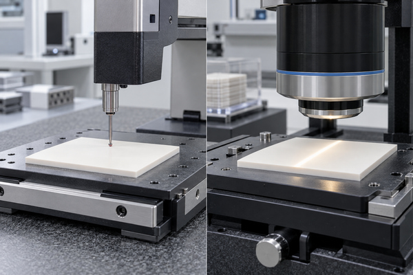
The two common approaches are contact profile measurement and non-contact areal measurement.
| Method | Strength | Limitation | Suitable use |
|---|---|---|---|
| Stylus profilometer | Established profile parameters and direct trace data | Tip geometry filters narrow valleys; direction matters; contact can be unsuitable for fragile coatings | Routine Ra or Rz inspection on accessible bare ceramic |
| Optical profilometer or interferometer | Captures an area without contact and shows texture distribution | Reflectivity, steep slopes, pores, scan size, and software filters can change the result | Polished substrates, thin films, process development, and Sa mapping |
| AFM | Very high vertical and lateral resolution over a small area | Small scan area may not represent a production substrate | Research and ultra-smooth surface characterization |
For repeatable inspection, measure multiple defined zones and record the raw setup. A single trace near an edge or visible defect should not represent the entire substrate unless the drawing explicitly defines that location as critical.
How Do As-Fired, Ground, Lapped and Polished Surfaces Differ?
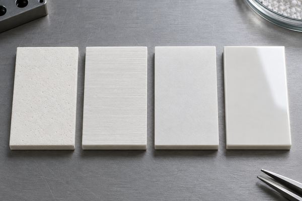
The finishing route changes both texture and cost. Ceramic surface finish also needs to be distinguished from the metal finish applied later: grinding or polishing controls the ceramic, while a plated finish controls the joining surface. Surface roughness of ceramics varies with the material grade and finishing route, which can also affect thickness tolerance, flatness, edge condition, and cleaning requirements.
| Surface condition | Typical texture | Main reason to select it | Buyer caution |
|---|---|---|---|
| As-fired | Process-dependent grain and pore texture | Thick-film circuits and applications without fine surface geometry | Lot consistency and open porosity may matter more than one average value |
| Ground | Directional machining marks | Thickness control, flatness improvement, or preparation for another process | Specify measurement direction relative to the grinding lay |
| Lapped | Lower, more uniform roughness with improved parallelism | Precision substrates and preparation for deposition or bonding | Lapping both sides can affect final thickness and cost |
| Polished | Very smooth surface with reduced peak height | Fine thin-film conductors, optical or semiconductor interfaces | Over-specification adds cost and may not improve thick-film or bonded-copper performance |
The correct choice is the least intensive finish that consistently supports the circuit and assembly process. Requiring mirror polishing on every ceramic PCB is not a reliability strategy.
What Is a Typical Ceramic Roughness Value?
There is no universal ceramic roughness value. Published substrate data show that some standard ceramic grades are supplied around Ra 0.4 micrometers, while fine alumina grades may be around Ra 0.1 micrometers. Alumina surface roughness therefore needs to be checked against the actual grade and surface condition. Polished products can be smoother. These values are product-specific examples, not automatic limits for another material, size, or process.
For our thin film ceramic PCB capability, the listed substrate roughness is Ra less than or equal to 0.1 micrometers, with special requirements down to Ra less than or equal to 0.05 micrometers. Feasibility still depends on material, substrate size, thickness, surface area, metallization stack, and the agreed inspection method.
Which Surface Condition Fits Thin-Film and Thick-Film Circuits?
Thin-film and thick-film processes do not need the same substrate texture.
| Circuit process | Roughness priority | Why it matters | Practical selection rule |
|---|---|---|---|
| Thin film | Low and uniform roughness, controlled defects | Supports continuous deposited films, fine photolithography, and narrow conductors | Define a polished or suitably lapped surface together with flatness and defect limits |
| Thick film | Compatible and repeatable surface, not necessarily mirror-polished | Fired paste behavior depends on paste chemistry, printing, firing, and substrate condition | Start with a qualified as-fired or processed grade; polish only when the design needs it |
Our thick film ceramic substrate examples use a different manufacturing route from thin film. Copying a thin-film roughness requirement into a thick-film drawing can increase cost without controlling the variables that actually determine print and firing quality.
How Does Surface Roughness Affect DPC, DBC and AMB Metallization?
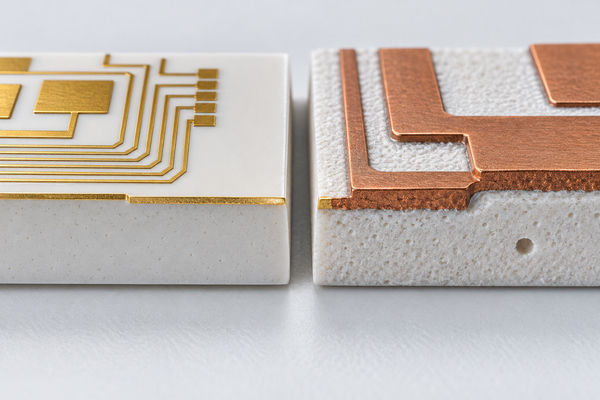
In DPC, the ceramic surface must support cleaning, seed-layer deposition, imaging, electroplating, and adhesion. Excessive peaks, pores, or contamination can reduce film continuity or create local thickness variation. A stable, process-qualified surface is more useful than chasing the lowest possible Ra.
For DBC and AMB, copper bonding is governed by the approved material system, surface preparation, bonding chemistry, temperature cycle, and interface quality. A thin-film polishing specification should not be imposed unless the bonded-copper process requires it. Our alumina DPC ceramic substrate is a relevant reference when the project needs plated copper patterns rather than fired paste or directly bonded copper.
What Changes for Wire Bonding, Die Attach and Soldering?
Assembly requirements often apply to the metallized surface rather than the bare ceramic. For wire bonding, pad metallurgy, pad roughness, hardness, contamination, and flatness are the immediate controls. Bare ceramic roughness matters upstream because it can affect the deposited metal, but a ceramic Ra certificate does not qualify a bond pad.
For die attach, local flatness, metallization planarity, void control, and attach-material thickness can be more important than average ceramic roughness. For soldering, the metal finish and solderable interface are the acceptance surfaces. Project documentation should identify the final joining process so the ceramic and metallization specifications are reviewed together.
Does Ceramic Surface Roughness Affect RF Performance?
At RF and microwave frequencies, conductor geometry and conductor-surface roughness are more direct loss variables than bare ceramic Ra. However, ceramic substrate surface roughness can influence deposited-metal continuity, line-edge definition, local conductor thickness, and photolithography yield.
Do not use bare ceramic Ra as a substitute for an RF model. Provide frequency, impedance, line width and spacing, conductor stack, substrate thickness, dielectric properties, and any insertion-loss target. The manufacturing review can then determine whether a smoother substrate or tighter metal-surface control is justified.
Which Surface Defects Are Not Roughness?
Cracks, scratches, dents, edge chips, open pores, glaze spots, contamination, and isolated pull-outs should not be hidden inside an Ra limit. Ra is an average and may remain acceptable even when a localized defect is functionally serious.
Control these conditions separately with visual criteria, allowable defect size and count, edge-quality requirements, inspection zones, and photographs or drawing notes. Ceramic surface roughness should be one part of the acceptance plan, not the entire surface-quality specification.
How Should Roughness Be Specified on a Ceramic Substrate Drawing?
Use the surface-texture symbol and callout convention required by the referenced drawing standard. The symbol alone does not define an Ra value, unit, manufacturing route, or inspection setup. A complete drawing callout should answer all of the following:
| Drawing item | What to state |
|---|---|
| Surface | Circuit side, back side, both sides, or a defined local zone |
| Condition | As-fired, ground, lapped, polished, or metallized |
| Parameter and limit | Ra, Rz, Sa, or another agreed parameter, including units and upper/lower limit |
| Standard | Applicable ISO, ASME, JIS, or customer method and revision |
| Measurement method | Stylus, optical, AFM, or an agreed equivalent |
| Settings | Cutoff/filter, evaluation length or scan area, trace direction, and tip/objective where relevant |
| Sampling | Number of substrates, zones per substrate, and pass/fail rule |
| Separate defects | Scratch, pore, chip, crack, contamination, and edge criteria |
If the required measurement length does not fit on the component, agree on a reduced evaluation method before production. Do not let the supplier choose an undocumented shortcut after inspection begins.
What Do We Need for a Ceramic Substrate RFQ?
Send the substrate material and grade, dimensions, thickness and tolerance, surface condition on each side, roughness parameter and limit, flatness or warpage requirement, metallization process, conductor stack, minimum line and space, surface finish, joining method, operating environment, quantity, and drawings. Include the measurement method and acceptance plan when roughness is function-critical.
At BSTCeramicPCB, we can review whether the requested finish matches thin film, thick film, DPC, DBC, AMB, RF, wire bonding, or die-attach requirements. Send us the drawing and application details at sales@bstceramicpcb.com for a manufacturability and quotation review.
 Products
 About us
 Contact us



