






















































 HOME
HOME

-

Ceramic PCB for Humanoid Robot joint actuators
2026 04,07 -
LTCC PCB Surprises: What Most People Miss
2025 12,09 -
Step-by-Step Guide to DPC PCB Design for Sensor Systems
2025 12,03 -
Ceramic PCBs Essential Benefits and Applications
2025 12,01 -
How Al2O3 DPC Ceramic Substrate PCB Enhances Heat Dissipation in Modern Electronics?
2025 11,28 -
How to Choose Between Ceramic, FR4, and Metal Core PCBs
2025 11,27 -
DPC Ceramic PCB Materials: Surprising Science Inside
2025 11,26 -
Wire bondable 2-layer Alumina substrates PCB | Bstceramic PCB
2025 09,22 -
Silicon Nitride Substrate, Silicon Nitride Ceramic Substrate Formula
2025 05,08 -
What is thick film ceramic PCB?
2023 08,02
How to Choose Gold Surface Finish in Ceramic PCB Design
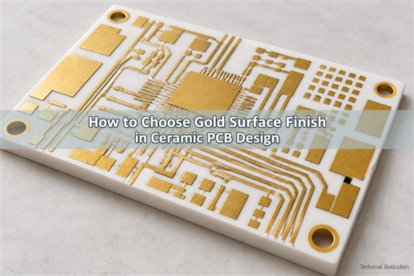
Choosing a gold surface finish in ceramic PCB design starts with the connection method: soldering, wire bonding, or repeated mechanical contact. ENIG is commonly used on solderable copper pads; ENEPIG can support soldering and qualified wire-bonding processes; soft gold serves qualified bonding applications; and hard gold serves wear-sensitive contacts. Gold in a thin-film or thick-film circuit may also form the conductor itself, rather than simply protect copper.
What Does Gold Do on a Ceramic PCB?
Gold provides an oxidation-resistant outer surface, but its function changes with the metal stack underneath. On ENIG-finished copper, the thin gold layer protects nickel before assembly. On a qualified bonding pad, the exposed gold becomes part of the bond interface. On a contact pad, its thickness and hardness influence wear life.
The ceramic is electrically insulating. Alumina or aluminum nitride must first receive an appropriate conductor and adhesion system; an ENIG specification does not describe how metal attaches to bare ceramic. Likewise, a gold-colored surface does not establish gold purity, thickness, or bondability.
Gold is not automatically necessary for every power substrate. Controlled bare-copper processing or a silver surface for a qualified sintering process may fit the assembly better. Select the joining interface first, rather than adding gold solely because it appears to be a premium option.
ENIG vs ENEPIG: Which Finish Fits the Assembly?
For copper-based ceramic circuits, compare ENIG vs ENEPIG against the actual soldering and bonding operations. The added palladium layer changes the interface; it does not make every bonding process interchangeable.
| Decision point | ENIG | ENEPIG |
|---|---|---|
| Stack above copper | Electroless nickel / immersion gold | Electroless nickel / electroless palladium / immersion gold |
| Common starting application | Flat, solderable pads | Mixed soldering and qualified wire-bonding interfaces |
| Gold wire bonding | Do not assume generic ENIG is suitable | A common candidate, subject to process qualification |
| Nickel corrosion control | Sensitive to nickel condition and immersion-gold process control | Palladium helps protect nickel during gold deposition; defects remain possible |
| Cost decision | Avoids an additional palladium process | Additional processing is justified when the assembly needs its interface properties |
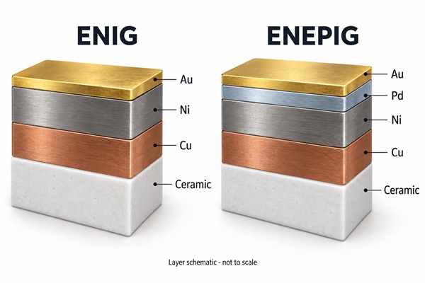
At BSTCeramicPCB, our nickel-palladium-gold DBC ceramic PCB combines a copper circuit with a separate Ni/Pd/Au finish. DBC describes the copper-to-ceramic construction; ENEPIG describes the exposed pad finish. Both need to appear in the specification.
Hard Gold vs Soft Gold: Which Surfaces Need Wear Resistance?
Use the contact mechanism to distinguish hard gold from soft gold. Repeated wiping is different from forming a permanent wire bond. A hard gold vs ENIG comparison is therefore primarily a comparison of contact duty and layer construction, not simply gold content.
| Surface | Appropriate consideration | Main limitation |
|---|---|---|
| Hard gold | Alloy-hardened gold for mating or sliding contacts | Hardening additions and deposit properties may conflict with wire bonding or soldering |
| Soft gold | High-purity, softer deposits for qualified bonding or joining processes | Less resistant to repeated abrasive contact |
| Immersion gold over nickel | Thin protective finish on solderable pads | Not a substitute for a specified wear-resistant contact deposit |
Hard gold plating thickness must be tied to contact force, travel, mating cycles, underplate, and environment. Do not increase thickness across the whole circuit when only a small contact region needs wear resistance. Selective finishes may be practical, but masking, electrical access for plating, and process compatibility must be resolved before layout release.
How Do Thin-Film and Thick-Film Gold Circuits Differ?
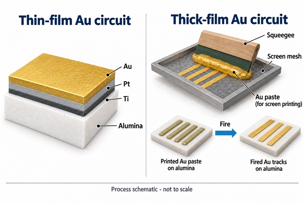
Thin-film and thick-film describe how a circuit's metallization is formed. ENIG and ENEPIG describe surface finishes. Treating these as equivalent alternatives can produce a drawing that specifies an outer surface but omits the conductor construction.
Thin-film circuits use deposited and patterned metal layers. An example is Ti/Pt/Au: titanium provides adhesion, platinum acts as a barrier, and gold provides the exposed conductive layer. Our thin-film ceramic circuits for wireless communication include this stack on alumina. The full patterned stack must preserve electrical isolation between separate traces.
Thick-film gold circuits use a formulated paste that is printed and fired. Paste chemistry, firing conditions, fired thickness, and ceramic compatibility affect adhesion and joining performance. A paste qualified for gold-wire bonding is not automatically qualified for every solder alloy or aluminum-wire process.
Our thin-film ceramic boards for medical electronics also use Ti/Pt/Au on alumina. For this construction, identify the deposited metal stack and intended joining process on the drawing; a gold-paste designation would describe a different fabrication route.
How Is Ceramic PCB Gold Plating Thickness Specified?
Specify each metal layer separately, including its minimum, maximum or tolerance, units, and measurement locations. A note reading only "gold PCB finish" cannot distinguish a thin immersion coating from a plated bonding layer or a fired gold conductor.
In ENIG, nickel is typically measured in several micrometers, while the immersion gold is much thinner. An illustrative range is 3-6 micrometers of nickel and 0.05-0.125 micrometers of gold; these are not universal acceptance limits. Use the agreed process specification and its applicable revision for production limits.
Check unit conversions before approving a drawing: 1 microinch equals 0.0254 micrometers, so 3 microinches is 0.0762 micrometers, not 3 micrometers. Confusing these units can change the gold requirement by almost forty times.
PCB surface finish thickness also needs a measurement plan. X-ray fluorescence can measure suitable multilayer deposits with appropriate calibration, but a thickness result alone does not demonstrate adhesion, solderability, or bond strength.
Can Gold-Finished Ceramic Pads Be Soldered?
Yes, when the finish stack and gold loading are compatible with the soldering process. During conventional tin-based soldering, the gold coating generally dissolves into the solder. A thick gold deposit combined with a small solder volume can produce an unfavorable gold concentration and brittle intermetallic phases.
For that reason, a thick soft-gold bonding pad should not automatically become a solder pad. Define separate pad functions where necessary, or qualify the shared finish with the actual solder alloy, solder volume, reflow profile, and required thermal exposure. Deliberately designed gold-tin die attachment is a different joining system and should not be evaluated as an ordinary tin-solder joint.
For PCB surface finish comparison, alternatives such as OSP, immersion tin, or immersion silver require their own conductor and assembly qualification. Their use on conventional copper PCBs does not prove compatibility with a particular ceramic metallization or high-temperature assembly sequence.
Which Gold Surfaces Support Wire Bonding?
Bondability depends on the complete deposited surface, cleanliness, roughness, hardness, underlayers, and bonding process. Qualified soft-gold and ENEPIG surfaces are common options, while generic hard-gold or ENIG callouts should not be treated as approval for gold wire bonding.
Specify the wire material and diameter, ball or wedge process, pad dimensions, and thermal history before selecting the finish. If solder reflow occurs before bonding, qualification must use pads that have experienced that reflow and the intended cleaning process. Testing pristine, as-plated samples alone can miss assembly-induced contamination or changes in the interface.
Use bond pull or shear testing appropriate to the bond type, and inspect the failure location. A passing force value does not explain whether failure occurred in the wire, at the bond interface, or by lifting the metallization. For loop geometry and bond-process details, see our guide to gold wire bonding on ceramic PCBs.
Does Gold Surface Finish Affect RF Performance?
Yes. At high frequencies, conductor loss depends on the complete stack, including nickel beneath a thin gold coating, surface roughness, conductor geometry, and operating frequency. Gold's resistance to oxidation does not mean that any gold-covered trace has low RF loss.
For loss-sensitive RF paths, compare the actual finished conductor stack in simulation or measured test structures. A microstrip result should not be transferred directly to a grounded coplanar waveguide with different current distribution. Nickel-free metallization may be worth evaluating, but it must still satisfy adhesion, diffusion-barrier, assembly, and reliability requirements.
Specify insertion-loss limits across the intended frequency range rather than approving a finish by its trade name. RF test coupons should reproduce the production stack and critical line geometry, including the finished conductor thickness.
What Finish Defects and Storage Risks Need Attention?
Investigate a failed joint by separating finish defects from assembly and handling problems. Adding more gold will not correct every weak bond or non-wetting pad.
| Observation | Possible contributors | Useful verification |
|---|---|---|
| Poor solder wetting | Contamination, storage exposure, incompatible finish or assembly process | Solderability testing using the intended alloy and thermal conditions |
| Weak or inconsistent wire bonds | Residue, unsuitable deposit properties, roughness or bonding settings | Pull/shear results together with failure-site inspection |
| Dark or irregular interface after joint failure | Possible nickel corrosion, other finish defects or process damage | Cross-section and interface analysis; color alone is insufficient |
| Metallization lifting or cracking | Adhesion loss, ceramic damage or thermomechanical stress | Cross-sections and tests after representative thermal exposure |
| Contact wear | Insufficient wear resistance, unsuitable underplate or excessive contact loading | Mating-cycle and contact-resistance testing |
Keep finished substrates in their specified clean packaging, avoid touching joining surfaces, and follow the supplier's storage and handling limits. Gold does not eliminate porosity, contamination, or damage to underlying layers. Unapproved abrasive cleaning can remove a very thin finish or change a bond surface.
How Should the Finish Be Defined on a Ceramic PCB Drawing?
Start with the pad function map, then assign the stack and acceptance criteria. A solder pad, a wire-bond pad, and a sliding contact can require different gold surface treatment even on the same ceramic substrate.
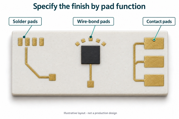
The fabrication drawing should identify the ceramic and conductor construction, finish boundaries, metal sequence, layer thickness limits, and areas that must remain unplated. It should also state the required inspection locations and reference the agreed finish specification. Do not use a general PCB surface finish types note in place of a defined layer stack.
Assembly requirements should identify soldering, wire bonding or contact duty; processing order; maximum thermal exposure; and the functional acceptance tests. For selective finishes, confirm that masking and plating access are compatible with the circuit pattern before the artwork is released.
The right gold surface finish in ceramic PCB design is the one that meets its joining, electrical, and wear requirements without unnecessary gold thickness or incompatible interfaces. At BSTCeramicPCB, we can review the proposed ceramic circuit construction and pad functions with you. Contact sales@bstceramicpcb.com to discuss the metallization needed for your design.
 Products
 About us
 Contact us



