






















































 HOME


-

Ceramic PCB for Humanoid Robot joint actuators
2026 04,07 -
LTCC PCB Surprises: What Most People Miss
2025 12,09 -
Step-by-Step Guide to DPC PCB Design for Sensor Systems
2025 12,03 -
Ceramic PCBs Essential Benefits and Applications
2025 12,01 -
How Al2O3 DPC Ceramic Substrate PCB Enhances Heat Dissipation in Modern Electronics?
2025 11,28 -
How to Choose Between Ceramic, FR4, and Metal Core PCBs
2025 11,27 -
DPC Ceramic PCB Materials: Surprising Science Inside
2025 11,26 -
Wire bondable 2-layer Alumina substrates PCB | Bstceramic PCB
2025 09,22 -
Silicon Nitride Substrate, Silicon Nitride Ceramic Substrate Formula
2025 05,08 -
What is thick film ceramic PCB?
2023 08,02
How to Solder Ceramic PCB Without Damaging the Pads?
Published:
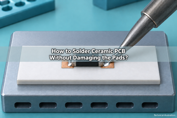
Before deciding how to solder ceramic PCB assemblies, identify the pad metallization: ordinary electronics solder joins the component termination to a compatible metal pad, not to bare ceramic. Use controlled heating across the board and measure the joint temperature. Increasing the iron setting alone can damage a thin conductor without solving poor heat transfer.
Confirm That the Pad Is Solderable
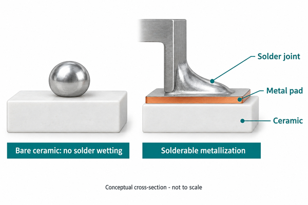
Ordinary electronics solder and flux do not wet bare alumina or aluminum nitride. A ceramic PCB needs a compatible metallized landing area. A surface that accepts wire bonding is not automatically qualified for the intended solder alloy and thermal cycle.
Start with the fabrication drawing or finish specification, not the pad color. Check the conductor material, finish stack, layer thicknesses, storage condition, and permitted assembly cycles.
| Board construction | What to establish before soldering | Main assembly concern |
|---|---|---|
| DPC copper circuitry, such as our alumina DPC circuit boards for LEDs | Final finish, copper thickness, pad adhesion, component land pattern | Fine pads can be damaged by prolonged contact or mechanical force |
| DBC copper circuitry, such as our DBC circuits for automotive components | Copper area and thickness, finish condition, substrate support | Large copper regions remove heat from a local joint |
| Fired conductor on our thick-film ceramic circuits | Exact paste system and its solderability and leach-resistance requirements | Some silver-based films can dissolve excessively during soldering |
| Thin-film or gold-finished circuit | Adhesion/barrier layers, gold thickness, solder compatibility | Thin layers and gold dissolution require a qualified process |
Match assembly requirements to the ordered finish; the ceramic material name alone is insufficient.
Why Does a Ceramic Board Need Different Heat Control?
A ceramic substrate and its metal pattern can conduct heat away from the joint faster than the same small pad on a conventional FR4 board. The actual response also changes with board thickness, copper coverage, fixtures, and any attached heat sink. Alumina and AlN boards should not automatically share one setup.
Local heating creates temperature gradients while the metal, solder, ceramic, and component expand differently. A hotter iron may overheat the contact area before the surrounding assembly warms sufficiently. Uniform preheating can reduce that imbalance, but its temperature must remain within the limits of every installed component and material.
Choose Hand Soldering, Reflow, or Controlled Rework
Use the process that can heat the intended connections without excessive exposure of neighboring parts. Accessibility and joint geometry matter as much as production quantity.
| Method | Appropriate use | Boundary to check |
|---|---|---|
| Temperature-controlled iron with preheating | Accessible terminals, wires, selected prototype joints | Tip contact area, thermal recovery, dwell limit, pad strength |
| Stencil printing and reflow | Repeated SMT placement and multiple joints | Paste volume, component limits, measured board profile |
| Controlled hot-air rework with bottom heating | Removing or replacing a suitable surface-mount component | Nozzle coverage, airflow, nearby parts, full joint melting before removal |
An ordinary iron is not a substitute for a validated process on hidden pads or a large power-device thermal attachment. Silver sintering, conductive adhesive bonding, and active-metal brazing are separate joining processes, not interchangeable solder pastes.
Select Solder Alloy and Flux Together
Choose the alloy from the component, conductor, service-temperature, and compliance requirements. Ceramic does not inherently require a special low-temperature solder, and a low melting point does not establish adequate operating-life performance.
| Alloy | Nominal melting behavior | Selection boundary |
|---|---|---|
| SAC305, Sn96.5Ag3Cu0.5 | Approximately 217-220 degrees C melting range | Common lead-free option where the finish and components allow its process window |
| Sn63Pb37 | 183 degrees C eutectic | Only for applications where leaded solder is permitted |
| Sn42Bi58 | 138 degrees C eutectic | Requires mechanical, service-temperature, and mixed-alloy compatibility assessment |
| Au80Sn20 | 280 degrees C eutectic | Specialized packaging with compatible metallization and controlled assembly equipment |
These are alloy melting temperatures, not recommended iron settings or oven peaks. Follow the selected solder product's processing data and the component's limits. The permissible process window is their overlap, not the highest temperature the ceramic can survive.
Use electronics-grade flux compatible with the finish and cleaning process. Plumbing flux is unsuitable. For silver-bearing thick-film pads, obtain the conductor supplier's approved solder system rather than assuming that any silver-containing alloy prevents leaching. For gold finishes, assess gold thickness relative to the solder volume and the underlying barrier layer.
Prepare the Board, Tools, and Support
Inspect the pads under magnification before applying heat. Record existing chips, cracks, contamination, or damaged metallization so that assembly defects are not confused with incoming damage.
- Disconnect power and use appropriate ESD protection, local fume extraction, and protection from hot surfaces.
- Clean with a method compatible with the finish, components, and coatings; do not abrade thin metal layers to make them appear brighter.
- Support the board flat without bending it or clamping tightly across a fragile edge. Account for the fixture's heat removal.
- Use a clean, tinned tip with sufficient contact area and thermal recovery for the joint. A needle tip can transfer heat poorly despite a high temperature setting.
- Have the solder, flux, component limits, thermocouples, and inspection criteria ready before the first joint.
Do not prescribe a generic bake cycle merely because the board is ceramic. Packaging instructions, absorbed moisture in components, contamination, and any polymer layers determine whether drying is needed and what cycle is allowed.
Establish and Measure the Preheat
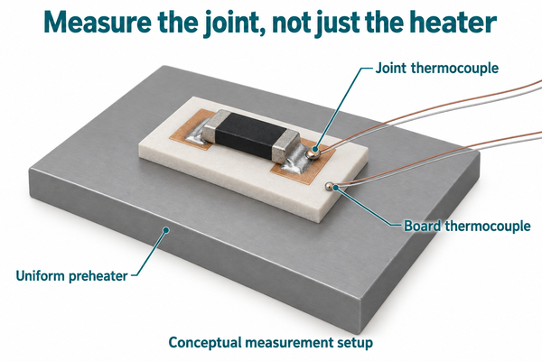
Preheat the supported assembly uniformly and verify the temperature on the board. A hot-plate display measures or controls the heater; it does not prove that the solder joint has reached the same temperature.
For a prototype, monitor a representative joint and a second location near a heat-sensitive component or cooler board region. Use a thermocouple attachment method that maintains thermal contact without interfering with the joint. Large assemblies may need more measurement points to identify the hottest and coldest locations.
Set the ramp, preheat level, peak, and cooling rate from the qualified component and solder limits. Record the measured trace. Stop if the required joint heating would exceed another component's exposure limit; change the fixture, heating method, or assembly sequence instead of raising the setting indefinitely.
How to Solder Ceramic PCB Terminals by Hand?
Hand solder only accessible joints with a defined temperature and dwell window. Start on a representative coupon or spare assembly when the metallization and heating response have not been proven.
- Stabilize the preheat. Confirm the board temperature and support before bringing the iron to the joint.
- Apply a controlled amount of flux. Keep it away from areas that must remain clean for later bonding or coating.
- Heat the pad and terminal together. Make gentle contact with the tinned tip; do not press against bare ceramic or scrape the conductor.
- Feed solder into the heated joint. Confirm wetting of both surfaces rather than melting a blob on the tip and depositing it onto a cold pad.
- Withdraw the solder and then the iron. Keep the component still while the joint solidifies.
- Inspect before continuing. If wetting fails within the established dwell limit, remove heat and diagnose the surface or heat-transfer problem. Repeated long attempts increase damage risk.
For a wire connection, provide strain relief outside the joint where the design allows it. A strong-looking solder fillet does not make a thin ceramic pad a mechanical anchor for cable movement.
Set Up Reflow From the Actual Assembly
Print the qualified paste volume, place components accurately, and profile the populated board in its production support. A profile from an empty board or a different copper pattern may not represent the final assembly.
Verify that the coldest relevant joint reaches the solder paste's required reflow conditions while the hottest component remains within its permitted exposure. Record ramp rate, peak temperature, time above liquidus, and cooling rate. Oven-zone settings are machine inputs; they are not the measured joint profile.
For exposed thermal pads, define stencil segmentation and solder volume from the package guidance and a prototype trial. Establish void acceptance and X-ray inspection requirements for the actual device instead of applying one universal void percentage to every ceramic PCB.
At BSTCeramicPCB, our ceramic PCB assembly service includes solder paste printing, SPI, SMT placement, reflow, and inspection. For a new ceramic construction, the relevant deliverable is a verified assembly process for that finish and BOM, not a copied oven recipe.
Cool, Clean, and Inspect Before Power-Up
Keep the assembly supported during controlled cooling. Avoid quenching a hot ceramic board or exposing it immediately to cold cleaning fluid. Once the assembly is within the cleaning process's permitted temperature range, remove residues when required by the flux and product specification.
Check wetting, bridges, component alignment, visible pad damage, and ceramic edges under magnification. Use X-ray for appropriate hidden-joint features and agreed void inspection; surface appearance alone cannot establish a hidden connection's quality.
Complete continuity, isolation, and functional checks before release. A successful electrical test does not rule out every microcrack or weak interface. For high-reliability assemblies, define the additional thermal-cycling or mechanical evaluation during prototype qualification.
Diagnose Failed Joints Before Reheating Them
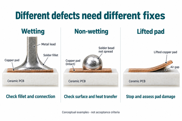
Separate a heat-transfer problem from an unsolderable or damaged surface. More temperature can worsen the latter two.
| Observation | What to check | Corrective direction |
|---|---|---|
| Solder melts on the tip but not at the connection | Tip contact, thermal recovery, copper area, fixture heat loss | Improve heat delivery and measured preheat within the process limits |
| Solder balls up on an intact pad | Finish identification, oxidation, contamination, flux compatibility | Verify solderability on a coupon before another attempt |
| Conductor thins or disappears | Thick-film composition, solder exposure, repeated heating | Stop; review leaching and the approved conductor/alloy combination |
| Pad edge lifts | Existing adhesion damage, tool pressure, premature component removal | Stop and assess repairability; solder cannot restore pad adhesion |
| Ceramic crack or edge chip appears | Support, local gradient, impact or bending | Isolate the assembly for engineering disposition |
| Hidden thermal joint has unacceptable voids | Paste deposition, profile, package geometry, outgassing | Revise and validate the process against device-specific acceptance criteria |
During rework, release the component only after all relevant joints are molten. Do not twist or pry it off. Record the thermal-cycle history and inspect the pads again before replacement; a universal allowed number of rework cycles cannot be assumed.
FAQ
Can a hole in a ceramic board be soldered like a plated FR4 hole?
Only if its specified metallization and geometry provide the required solderable connection. A drilled ceramic hole may be unplated, and a filled via is not automatically a lead-insertion hole. Check the drawing before inserting or soldering a wire.
Is soldering a ceramic capacitor the same as soldering a ceramic PCB?
No. A ceramic capacitor is a component with its own termination and thermal-shock restrictions. Those limits still apply when it is mounted on a ceramic PCB; the substrate's temperature capability does not override them. Avoid direct tip contact with the capacitor body.
Can solder repair a cracked ceramic substrate?
No. Solder may connect exposed metal, but it does not restore the ceramic's mechanical integrity or insulation. A cracked substrate needs an engineering disposition, not a larger solder fillet.
Qualify the Joint Before Scaling Production
When evaluating how to solder ceramic PCB assemblies for production, verify the solderable finish, measured heating, and acceptance criteria for the connection. Validate those conditions on a representative prototype before repeating the process across a batch.
For an assembly quotation, send us the board drawing, metallization and finish stack, BOM, placement data, quantity, and inspection requirements at sales@bstceramicpcb.com. We can review the ceramic circuit and assembly requirements together rather than selecting a soldering process from the substrate name alone.
 Products
 About us
 Contact us



