






















































 HOME
HOME

-

Ceramic PCB for Humanoid Robot joint actuators
2026 04,07 -
LTCC PCB Surprises: What Most People Miss
2025 12,09 -
Step-by-Step Guide to DPC PCB Design for Sensor Systems
2025 12,03 -
Ceramic PCBs Essential Benefits and Applications
2025 12,01 -
How Al2O3 DPC Ceramic Substrate PCB Enhances Heat Dissipation in Modern Electronics?
2025 11,28 -
How to Choose Between Ceramic, FR4, and Metal Core PCBs
2025 11,27 -
DPC Ceramic PCB Materials: Surprising Science Inside
2025 11,26 -
Wire bondable 2-layer Alumina substrates PCB | Bstceramic PCB
2025 09,22 -
Silicon Nitride Substrate, Silicon Nitride Ceramic Substrate Formula
2025 05,08 -
What is thick film ceramic PCB?
2023 08,02
What is resistance on Thick film ceramic PCB? How to print it?
The black rectangular areas commonly seen as resistance on Thick film ceramic PCB are printed thick-film resistors. They are not separate SMD components or ordinary black ink. We form them by screen-printing a functional resistor paste onto the ceramic, drying and firing the deposit, measuring the fired value and, when tighter tolerance is required, laser-trimming the resistive film.
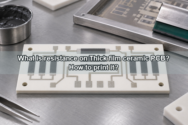
What Are the Black Areas on a Thick Film Ceramic PCB?
The black areas are fired resistive films positioned between conductor terminations. Current enters through one termination, passes through the resistive film and leaves through the other termination. The paste chemistry and the geometry of this path establish the nominal resistance.
Because the resistor is printed directly on the substrate, it becomes part of the thick-film ceramic circuit. It has no separate ceramic chip body, end caps or solder joints. This distinction matters when an engineer specifies artwork, material compatibility, firing order, trim access and final testing.
A printed resistor is also different from a printed conductor. A conductor is intended to carry current with low loss; a resistor is formulated and shaped to create a controlled voltage drop or heat output. Its dark appearance alone does not identify its electrical value.
Why Use a Printed Resistor Instead of an SMD Resistor?
A printed resistor is useful when integrating the resistance into the ceramic circuit provides a clear design benefit. It can save component area, eliminate selected solder joints, support custom geometries and allow the value to be adjusted on the substrate by laser trimming. Short printed interconnections can also help where parasitic effects are important.
It is not automatically better than an SMD resistor. A discrete component is easier to replace, is available in standardized values and packages, and may be preferable when field service or second sourcing is important.
| Decision factor | Printed thick-film resistor | Discrete SMD resistor |
|---|---|---|
| Integration | Formed directly on the ceramic circuit | Mounted as a separate component |
| Value options | Geometry and paste family can be customized | Selected from standard component values |
| Final adjustment | Can be laser-trimmed after firing | Normally replaced with another value |
| Interconnections | No resistor-body solder joints | Requires pads and attachment joints |
| Serviceability | Not field-replaceable | Can be replaced during repair |
| Typical fit | Hybrid circuits, sensors, resistor networks and custom functions | General-purpose circuits and standardized assemblies |
The correct choice depends on tolerance, power, available area, qualification requirements, production volume and service strategy.
What Is Thick-Film Resistor Paste Made Of?
Thick-film resistor paste normally contains three functional parts before firing:
- a resistive phase, commonly based on ruthenium oxide or related ruthenate systems;
- glass frit, which helps form the fired matrix and bond the film to the ceramic;
- an organic vehicle, which provides the viscosity and screen-printing behavior needed before firing.
During drying, volatile components leave the deposit. During firing, the remaining organic material is largely removed, the glass phase softens and bonds to the substrate, and the resistive particles form the electrical network that determines the fired behavior. The black layer is therefore a functional ceramic-compatible material system, not decorative ink.
Paste selection is not based on color. We select a compatible resistor decade and material family according to the target sheet resistance, TCR, conductor system, substrate, firing atmosphere, power loading and stability requirement. A paste qualified on one substrate and conductor stack should not be transferred to another without validation.
How Is the Printed Resistance Value Formed?
For a simple rectangular resistor, the first-order relationship is:
R = Rs x L / W
Here, R is the nominal resistance, Rs is the fired sheet resistance in ohms per square, L is the effective resistor length and W is its width. The ratio L/W is the number of squares. With the same paste, a longer path increases resistance and a wider path reduces resistance.
For example, a resistor that is twice as long as it is wide contains approximately two squares. A 10 kOhm/square paste would therefore give a first-order design value near 20 kOhm. This is a starting calculation, not the final production result.
| Design input | Effect on the resistor | Manufacturing consideration |
|---|---|---|
| Paste sheet resistance | Sets the basic resistance range | Use fired data for the selected substrate and profile |
| Length | A longer path generally raises resistance | Include termination and trim geometry |
| Width | A wider path generally lowers resistance | Very narrow prints are more sensitive to edge variation |
| Fired thickness | Changes the effective resistive network | Control screen construction and print consistency |
| Conductor overlap | Affects current entry and effective length | Keep overlap and registration repeatable |
| Trim allowance | Provides room for upward adjustment | Preserve a stable current path after trimming |
End effects, print-edge shape, conductor overlap and process spread require compensation beyond the ideal L/W equation.
How Do You Print a Thick-Film Resistor on Ceramic?
A typical manufacturing sequence is:
- Prepare the ceramic substrate. Confirm material, thickness, surface condition, dimensions and cleanliness.
- Print and fire the conductor terminations. Establish a compatible electrical interface for the resistor.
- Prepare the resistor screen and paste. Control artwork, mesh, emulsion, storage, mixing and working life.
- Screen-print the resistor pattern. Control registration, squeegee pressure, speed, angle, snap-off and substrate support.
- Level and dry the print. Allow the deposit to settle and remove volatile material under the qualified conditions.
- Fire the resistor. Use the approved furnace profile for the complete paste, conductor and substrate system.
- Measure the as-fired resistance. Record the value before adjustment.
- Laser-trim where required. Increase the value toward the specified target while monitoring resistance.
- Apply overglaze when specified. Protect the resistor while accounting for any additional thermal-cycle effect.
- Perform final electrical and visual inspection. Verify value, trim condition, print quality and specified reliability requirements.
This order can change with the material system and layer stack. A qualified process sequence, rather than one universal recipe, must govern production.
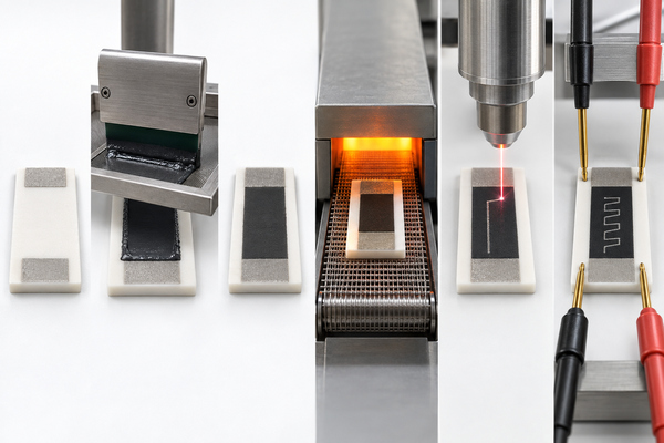
Why Is High-Temperature Firing Necessary?
Screen printing only deposits the wet geometry. Firing creates the functional resistor. A controlled firing profile removes the organic vehicle, softens the glass phase, bonds the film to the ceramic and develops a stable resistive network.
Many conventional thick-film resistor systems use a peak near 850 degrees C, but this is not a universal setting. Peak temperature, dwell, belt speed, furnace atmosphere, heating and cooling rates, and the number of refires are paste-specific. The supplier's approved profile and the complete conductor-resistor stack must be evaluated together.
An incorrect profile can shift resistance and TCR, weaken adhesion or increase lot-to-lot variation. This is why firing is an electrical manufacturing step, not simply a drying operation.
Why Does Actual Resistance Differ from the Calculated Value?
The L/W calculation assumes an ideal uniform film. Actual resistance also depends on:
- paste sheet-resistance variation and lot behavior;
- wet and fired film thickness;
- screen wear, print edges and local pinholes;
- conductor-resistor overlap and registration;
- substrate surface condition and flatness;
- firing peak, dwell, atmosphere and refiring history;
- measurement temperature, probe placement and contact resistance.
We use process compensation and trial data to position the as-fired result within a practical trim window. Where laser trimming is planned, the untrimmed resistor is normally designed below the final target because removing resistive material increases resistance. If the fired value is already above target, the same trimming process cannot restore it downward.
How Does Laser Trimming Set the Final Resistance?
Laser trimming removes a controlled portion of the fired resistive film while the value is measured. The cut lengthens or constricts the current path, increasing resistance toward the target. Straight, L-shaped, plunge and serpentine cuts may be selected according to resistor geometry, adjustment range and power distribution.
The cut must not sever the electrical path or create an unstable narrow neck. Trim position, remaining resistor width, current density and local heating all affect long-term performance. After trimming, we remeasure the value and inspect the cut for debris, cracks and damage to adjacent conductors.
Our published thick-film reference capability includes resistance values from 40 mOhm to 1000 MOhm, functional laser trimming, +/-2% absolute resistor accuracy and +/-0.1% ratio accuracy. These are capability references rather than universal guarantees. Achievable results still depend on paste family, value range, geometry, power, TCR and test conditions.
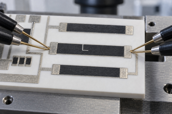
How Is a Printed Thick-Film Resistor Measured?
Resistance is normally measured after firing to establish the as-fired value, during trimming to control the adjustment, and again after trimming or final processing to verify acceptance. The measurement temperature, settling time, probe location and instrument method should be defined for repeatable results.
For moderate and high resistance values, an appropriate resistance meter or automated probe tester may be sufficient. For low-ohmic printed resistors, a two-wire reading can include lead resistance, probe resistance and contact resistance. A four-wire Kelvin method separates the force and sense paths so these unwanted series resistances have much less influence on the reported value.
Electrical measurement should be paired with visual inspection. Registration, edge definition, pinholes, conductor overlap, fired-surface condition and laser-cut quality can reveal risks that one room-temperature resistance reading cannot show.
How Are Tolerance, TCR and Stability Controlled?
Initial tolerance, ratio tolerance and TCR describe different requirements. Initial tolerance limits the measured value at a stated condition. Ratio tolerance controls the relationship between matched resistors. TCR, expressed in ppm/degree C, describes how resistance changes over a specified temperature range.
| Requirement | What it defines | Information needed on the drawing |
|---|---|---|
| Nominal resistance | Required electrical value | Value for every printed resistor |
| Initial tolerance | Allowed error at the test condition | Percentage or absolute limit and test temperature |
| Ratio tolerance | Matching between selected resistors | Resistor group and permitted ratio error |
| TCR | Resistance change with temperature | ppm/degree C limit and temperature interval |
| Stability | Permitted drift after exposure or use | Test condition, duration and acceptance limit |
As-fired resistors normally have a wider distribution than resistors adjusted by laser trimming. Trimming can tighten the room-temperature value, but it does not automatically guarantee the required TCR, load-life drift or thermal-cycle performance. Those characteristics depend on the material system, geometry, process and validation plan.
How Much Power Can a Printed Resistor Handle?
Nominal resistance alone does not define power capability. Resistor area, aspect ratio, power density, maximum voltage, ceramic thermal conductivity, conductor heat spreading, mounting interface, ambient temperature and nearby heat sources all affect film temperature.
Two resistors with the same ohmic value can have very different power limits if their printed areas or heat paths differ. Local current crowding at conductor overlaps or laser-trim cuts can also create hot spots. For this reason, a power requirement should include continuous and peak load, duty cycle, working voltage, ambient or substrate temperature and the actual mounting condition.
The ceramic substrate can spread heat, but it does not make every printed resistor suitable for unrestricted high-temperature or high-power use. Thermal and electrical limits must be verified for the specific design.
Where Are Printed Thick-Film Resistors Used?
Printed resistors are selected when substrate-level integration, custom geometry or final trimming supports the circuit function.
- Automotive level sensing: a long resistive track and moving contact can convert fuel or oil level into an electrical signal. Our thick-film ceramic substrate for automotive fuel gauges is relevant to this integrated resistive-track architecture.
- Oil-level and fluid sensing: a thick-film ceramic substrate for an automotive oil-level sensor requires the resistor, contact system, fluid exposure and mechanical reference to be evaluated together.
- Medical and precision sensor circuits: trimmed networks can set gain, bias or bridge balance. An Al2O3 thick-film ceramic substrate for medical equipment can integrate printed conductors and resistors on one stable base.
- Industrial and power electronics: printed resistors can provide sensing, discharge, current limiting or voltage-divider functions close to other thick-film circuit elements.
- Heating and temperature control: a designed resistive path can generate heat, but power density, temperature uniformity and the control method must be specified separately from nominal resistance.
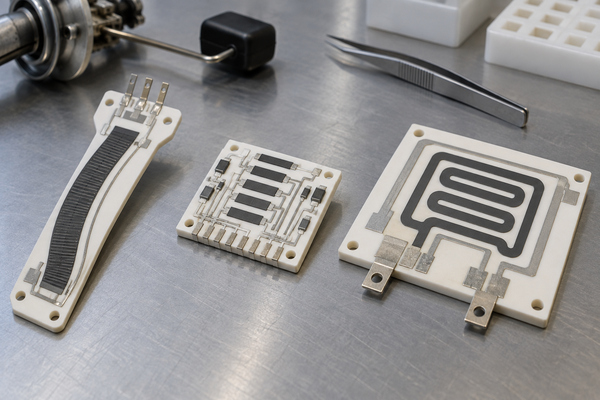
What Information Is Needed for Manufacturing and Quotation?
We review each printed resistor as part of the complete material and firing stack for a custom thick-film ceramic PCB. A useful manufacturing package should include:
- ceramic material, thickness, outline, holes and dimensional tolerances;
- conductor, resistor, dielectric and overglaze artwork in the intended firing order;
- nominal value, initial tolerance, ratio matching and TCR for each resistor;
- fixed resistor dimensions or available layout area;
- continuous and peak power, duty cycle, maximum voltage and operating temperature;
- laser-trim target, trim allowance and measurement condition;
- mounting, heat path and environmental exposure;
- reliability tests, traceability level, prototype quantity and production volume.
We review material compatibility, printable geometry, conductor overlap, firing sequence, trim access, power density and test method before quotation. A resistance value by itself is not enough to define a repeatable printed component. Send the drawing package to sales@bstceramicpcb.com so our engineers can evaluate the resistance on Thick film ceramic PCB against the actual design conditions.
 Products
 About us
 Contact us



