






















































 HOME


-

Ceramic PCB for Humanoid Robot joint actuators
2026 04,07 -
LTCC PCB Surprises: What Most People Miss
2025 12,09 -
Step-by-Step Guide to DPC PCB Design for Sensor Systems
2025 12,03 -
Ceramic PCBs Essential Benefits and Applications
2025 12,01 -
How Al2O3 DPC Ceramic Substrate PCB Enhances Heat Dissipation in Modern Electronics?
2025 11,28 -
How to Choose Between Ceramic, FR4, and Metal Core PCBs
2025 11,27 -
DPC Ceramic PCB Materials: Surprising Science Inside
2025 11,26 -
Wire bondable 2-layer Alumina substrates PCB | Bstceramic PCB
2025 09,22 -
Silicon Nitride Substrate, Silicon Nitride Ceramic Substrate Formula
2025 05,08 -
What is thick film ceramic PCB?
2023 08,02
What Is Sheet Resistance? Ohms per Square, Calculation and Measurement
Published:
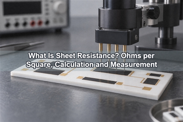
Sheet resistance describes how strongly a uniform conductive or resistive film opposes current flowing along its surface. It is reported in ohms per square, abbreviated as Ω/sq. For an ideal uniform film, the value combines bulk resistivity and film thickness, so engineers can compare a film system without tying the result to one particular square size.
What Is Sheet Resistance?
Sheet resistance is the resistance of a thin, nominally uniform layer normalized to a square geometry. It is useful for conductive films, resistive films, semiconductor layers and printed resistor materials because current flows mainly in the plane of the layer. The symbol is commonly Rs.
For a material with volume resistivity ρ and uniform thickness t:
Rs = ρ / t
The units must be consistent. If ρ is in Ω·cm and t is in cm, Rs is in Ω/sq. The inverse conversion is ρ = Rs × t. Conductivity is σ = 1/ρ, so thickness is still required when converting sheet resistance to conductivity.
Why Is Sheet Resistance Measured in Ohms per Square?
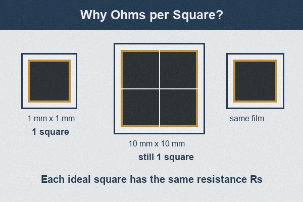
A square of uniform film has the same ideal resistance between two opposite full-width edges regardless of whether the square is 1 mm or 10 mm wide. Scaling the square makes the current path longer, which raises resistance, but also makes the path wider, which lowers resistance by the same ratio. That is why the sheet resistance unit is written as ohms per square instead of ohms per millimetre.
The word “square” is not a physical area unit. It indicates the geometry used to normalize an in-plane electrical measurement. We use the plain-text abbreviation Ω/sq here to avoid confusing the traditional hollow-square notation with a missing-character box.
Sheet Resistance vs Resistance and Resistivity
| Quantity | What it describes | Typical unit | Geometry dependence |
|---|---|---|---|
| Resistance, R | A specific component or path | Ω | Depends on length, width, thickness and contact geometry |
| Sheet resistance, Rs | A uniform film normalized to one square | Ω/sq | Independent of the absolute size of an ideal square |
| Resistivity, ρ | A bulk material property | Ω·m or Ω·cm | Independent of sample geometry when the material is uniform |
The distinction between resistivity and sheet resistance matters whenever thickness changes. Two films made from the same bulk material can have different sheet resistance if their thicknesses differ. Conversely, two films can have the same sheet resistance while using different combinations of resistivity and thickness.
Sheet Resistance Formula
For a rectangular film with uniform thickness and full-width equipotential contacts at the two ends:
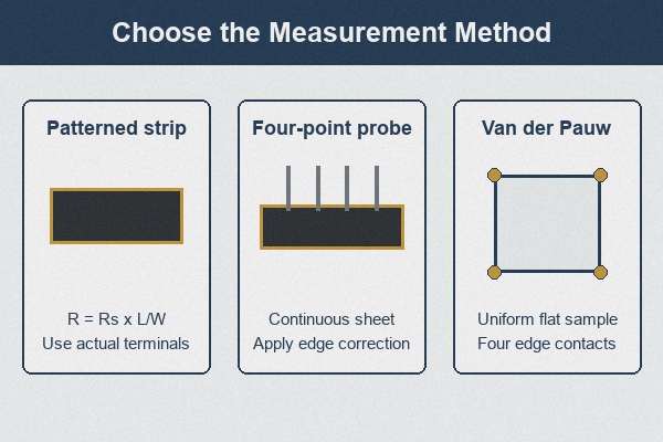
R = ρL / (Wt) = Rs × (L/W)
The ratio L/W is the number of squares, often written as N. Therefore:
R = Rs × N and Rs = R / N
This sheet resistance formula is a first-order model for a uniform straight film. Corner current crowding, narrow terminals, nonuniform thickness, laser-trim cuts and edge damage can make the effective number of squares differ from the simple artwork ratio.
How to Calculate Resistance from Sheet Resistance?
- Identify the active electrical length between the two terminations.
- Identify the active film width in the same unit.
- Calculate the number of squares: N = L/W.
- Multiply the specified sheet resistance by N.
- Review terminal overlap, corners, trim allowance and process tolerance before releasing the value.
A serpentine path can be divided into straight sections for an initial estimate, but bends and junctions require geometry correction or empirical characterization. A calculation should not be used as final acceptance data for a patterned resistor without an agreed test method.
A sheet resistance to resistance conversion always needs geometry. A sheet resistance calculator can automate the number-of-squares calculation and unit conversion, but it cannot choose the correct edge correction, contact model or acceptance method for the design.
Sheet Resistance Calculation Example
Assume a uniform resistor film is specified at 100 Ω/sq. Its active length is 6 mm and its width is 2 mm:
N = 6 / 2 = 3 squares
R = 100 Ω/sq × 3 = 300 Ω
If the same material is printed as a 2 mm × 2 mm square, the ideal end-to-end resistance is 100 Ω. If its fired thickness changes while bulk resistivity remains constant, the sheet resistance changes inversely with thickness. In real thick-film ceramic circuits with integrated resistors, paste system, fired thickness, terminations, substrate interaction and trim geometry must be controlled with the drawing and approved sample.
How Does a Four-Point Probe Measure Sheet Resistance?
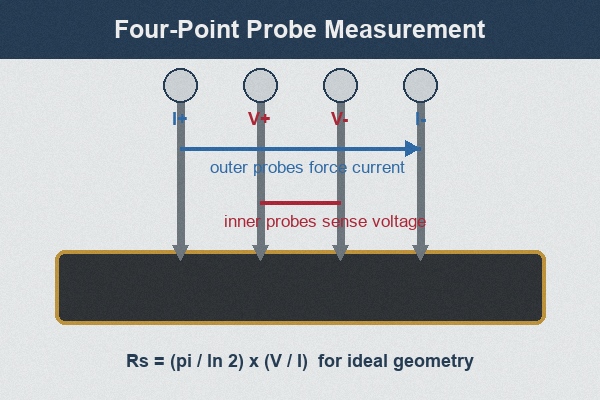
A four-point probe separates current injection from voltage sensing. The two outer probes drive a known current through the film, while the two inner probes measure voltage. Because almost no current flows through the voltage-sense circuit, lead and contact resistance have much less influence than in a two-probe measurement.
For an effectively infinite sheet with equal probe spacing and negligible edge effects:
Rs = (π / ln 2) × (V/I) ≈ 4.5324 × (V/I)
This relation needs a correction factor when the sample is finite, close to an edge, unusually thick relative to probe spacing or otherwise outside the ideal geometry. A four point probe sheet resistance result should therefore include sample geometry, probe spacing, current, temperature and the correction method.
A dedicated sheet resistance meter may combine a source, voltmeter, probe head and correction software. For suitable continuous conductive films, non contact sheet resistance measurement based on eddy-current or related methods can avoid probe marks, but the material range, thickness and calibration still have to match the instrument.
When Should You Use the Van der Pauw Method?
The Van der Pauw method is useful for a flat, uniformly thick sample when four sufficiently small contacts can be placed around its perimeter. It is especially valuable when the sample is not a long rectangular strip. Two characteristic resistances are measured in orthogonal configurations, and sheet resistance satisfies:
exp(-πRA/Rs) + exp(-πRB/Rs) = 1
If RA and RB are equal, the expression reduces to Rs = (π/ln 2)R. The method assumes a simply connected sample without isolated holes, uniform thickness and suitable edge contacts. It is not a direct substitute for measuring a narrow finished resistor between its actual terminations.
What Causes Sheet Resistance Measurement Errors?
| Source | Why it changes the result | Control to record |
|---|---|---|
| Edge proximity and sample size | Current distribution no longer matches the infinite-sheet assumption | Dimensions, probe location and correction factor |
| Film nonuniformity | Local thickness or composition changes create position-dependent values | Measurement map and sampling plan |
| Probe contact or damage | Poor or unstable contact adds noise; excessive force can mark the film | Probe type, force and repeatability |
| Temperature and self-heating | Material resistance changes with temperature | Test temperature, current and dwell time |
| Pattern and terminal geometry | Narrow pads, corners and trim cuts alter current flow | Dedicated coupon or component test method |
| Instrument range and polarity | Low signals, offsets and thermoelectric voltage can bias V/I | Range, current reversal and uncertainty |
The phrase sheet resistance correction factor refers to a geometry-dependent correction, not one universal number. The selected method must match the sample shape and the electrical question being answered.
How Is Sheet Resistance Used in Ceramic Circuits?
In thick-film ceramic circuits, resistor pastes are commonly identified by a nominal fired sheet-resistance family. The artwork then sets the initial number of squares, while printing, drying, firing, conductor overlap and laser trimming determine the delivered component resistance. Sheet resistance is therefore an input to geometry design, not a complete finished-resistor specification.
In thin-film ceramic PCB fabrication, deposited film thickness and pattern definition affect both conductor and resistor performance. The appropriate measurement may be a witness coupon, a four-terminal test structure or the finished element between defined pads. The choice depends on whether the objective is material characterization, process monitoring or component acceptance.
We manufacture custom thick-film and thin-film ceramic circuits. For resistor-bearing designs, our engineering review connects the target value with the film system, geometry, terminations, trim allowance, temperature requirement and test points. We do not replace these drawing conditions with a generic Ω/sq value.
What Should Your Ceramic Circuit Drawing Specify?
- Target resistance or sheet-resistance family, including units.
- Active length, width, terminations and any excluded edge region.
- Film type and approved material system, when already selected.
- Initial tolerance, final tolerance and laser-trim allowance.
- Test temperature, test current or voltage, and settling time.
- Required TCR, power, voltage and environmental limits.
- Measurement method, correction factor and sampling plan.
- Witness coupon or dedicated test structure requirements.
For a custom thick-film ceramic circuit, send us the circuit drawing, target values, tolerance, material preference, operating conditions and quantity. We can review whether the requested sheet-resistance range, geometry and inspection method form a consistent manufacturing specification before production planning.
Sheet Resistance FAQs
Is Ω/sq dimensionally different from Ω?
No. The square is a geometry label rather than another physical dimension. It prevents a film-normalized value from being mistaken for the resistance of an arbitrary component.
Can a multimeter measure sheet resistance directly?
A two-lead multimeter can measure the end-to-end resistance of a defined strip, but contact and lead resistance remain in the result. For low-resistance films or material characterization, four-terminal methods are usually more appropriate.
Does a lower sheet resistance always mean a better film?
No. The required value depends on whether the film is a conductor, resistor, heater, sensor or electrode. Uniformity, adhesion, TCR, power density and stability may matter as much as the nominal Ω/sq value.
Can sheet resistance predict a laser-trimmed resistor exactly?
No. It provides the starting geometry model. The final result also depends on terminal overlap, the effective current path, trim shape, process variation and the defined measurement conditions.
When the purpose is a ceramic resistor or conductive-film design, sheet resistance should be tied to the actual film, thickness, geometry and test method. Contact BSTCeramicPCB at sales@bstceramicpcb.com with your drawing and electrical requirements for an engineering review.
 Products
 About us
 Contact us



