






















































 HOME
HOME

-

Ceramic PCB for Humanoid Robot joint actuators
2026 04,07 -
LTCC PCB Surprises: What Most People Miss
2025 12,09 -
Step-by-Step Guide to DPC PCB Design for Sensor Systems
2025 12,03 -
Ceramic PCBs Essential Benefits and Applications
2025 12,01 -
How Al2O3 DPC Ceramic Substrate PCB Enhances Heat Dissipation in Modern Electronics?
2025 11,28 -
How to Choose Between Ceramic, FR4, and Metal Core PCBs
2025 11,27 -
DPC Ceramic PCB Materials: Surprising Science Inside
2025 11,26 -
Wire bondable 2-layer Alumina substrates PCB | Bstceramic PCB
2025 09,22 -
Silicon Nitride Substrate, Silicon Nitride Ceramic Substrate Formula
2025 05,08 -
What is thick film ceramic PCB?
2023 08,02
What Is a Thick Film PCB? Materials, Process and Applications
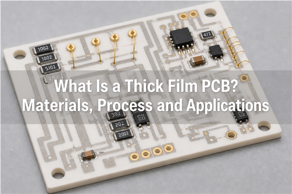
A thick film pcb forms conductors, resistors, and dielectric features by screen-printing engineered pastes onto a ceramic substrate and firing them into stable functional layers. It is useful when a compact circuit must tolerate heat, integrate printed functions, or operate where an organic laminate is a weak fit. The term describes the deposited circuit technology, not the overall board thickness.
What Is a Thick Film PCB?
A thick film PCB is usually a fired ceramic circuit rather than a conventional laminated PCB. A patterned screen transfers metal, resistor, or dielectric paste onto a fired ceramic tile. After leveling and drying, the print is fired so its functional material bonds to the ceramic. Additional print-and-fire cycles can add resistors, crossovers, insulation, overglaze, and attachment pads.
“Thick film” should not be confused with a thick copper PCB. A thick copper board uses heavy copper foil or plated copper on an organic or ceramic stack. Thick film uses a paste containing functional particles, glass or another binder system, and organic vehicles that are removed during firing. DBC, AMB, and DPC are separate metallization technologies even when their finished copper is physically thicker.
How Is a Thick Film PCB Structured?
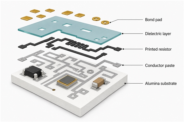
The simplest structure has a ceramic base and one fired conductor layer. More capable circuits add printed resistors between conductor terminals, dielectric layers beneath crossovers, protective overglaze, backside circuitry, or filled vias. Semiconductor dies, passive components, connectors, and wire bonds can then be attached to suitable pads.
| Element | Function | Design consequence |
|---|---|---|
| Ceramic substrate | Provides insulation, mechanical support, and a thermal path | Material, thickness, surface finish, flatness, and hole quality affect the complete circuit |
| Fired conductor | Creates traces, pads, terminations, and bonding areas | Paste selection controls conductivity, solderability, wire bonding, and migration resistance |
| Printed resistor | Integrates resistance, sensing, heating, or voltage division | Geometry, firing history, power density, and laser trim determine the final value |
| Dielectric or overglaze | Insulates crossovers and protects selected features | Pinholes, print registration, and expansion compatibility are critical |
| Attached components | Add active devices and functions not practical to print | Pad finish and assembly temperature must match the conductor system |
Which Materials Are Used in Thick Film PCBs?
The substrate and paste system must be selected together. A conductor that performs well on 96% alumina may need different firing, adhesion, or atmosphere controls on aluminum nitride. The number of planned firing cycles also matters because each later cycle can change earlier layers.
| Material | Typical role | Selection boundary |
|---|---|---|
| 96% alumina | General-purpose thick film ceramic substrate | Widely supported and economical; a strong default for hybrid circuits, sensors, and printed resistors |
| High-purity alumina | Smoother, more tightly controlled ceramic base | Useful when surface quality, dielectric performance, or finer geometry justifies the added cost |
| Aluminum nitride | Higher-conductivity ceramic for concentrated heat | Requires a paste, atmosphere, and firing process proven for the selected AlN grade |
| Ag, Ag/Pd, Au, or Pt/Au pastes | Conductive traces and attachment pads | Choose for conductivity, solder leach resistance, wire bonding, migration risk, temperature, and cost |
| RuO2-based resistor paste | Printed resistors and resistor networks | Target sheet resistance, TCR, trim range, dimensions, and power density must be specified together |
| Glass dielectric or overglaze | Insulation, crossover support, and environmental protection | Must be compatible with the conductor, ceramic, firing profile, and operating voltage |
Alumina remains the workhorse material for thick-film electronics. Published thick-film alumina substrate guidance also shows why ceramic grade, thickness, hole size, surface condition, and edge finishing should be treated as manufacturing inputs rather than incidental drawing notes.
How Is a Thick Film PCB Manufactured?
- Prepare the ceramic. Laser cutting, drilling, scribing, or other ceramic machining is completed at the stage selected for the product. The surface is cleaned so paste can wet and bond consistently.
- Print the first conductor. A stainless-steel screen, emulsion opening, squeegee, paste rheology, and snap-off setting define the wet pattern.
- Level and dry the print. Controlled leveling allows the paste to settle. Drying removes solvents without blistering or distorting the pattern.
- Fire the conductor. A belt furnace removes the organic vehicle and develops the fired bond. Many conventional air-fired systems use a peak near 850°C, but the exact profile is specific to the paste and substrate.
- Repeat for other functions. Resistors, dielectrics, crossovers, backside conductors, and overglaze are printed and fired in a controlled sequence.
- Trim and finish. Printed resistors can be measured and laser trimmed. Suitable pads may be plated or otherwise finished for soldering, brazing, die attach, or wire bonding.
- Inspect and test. Registration, conductor continuity, isolation, resistor value, adhesion, geometry, flatness, and visual defects are checked before assembly.
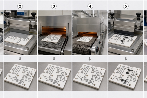
A single “firing temperature” is not enough to reproduce a process. For example, DuPont publishes a 30-minute cycle with an 850°C peak and a 10-minute peak dwell for one gold conductor, while other formulations use different meshes, dry conditions, thicknesses, and profiles. The safe rule is to qualify the complete paste-substrate-profile combination.
What Can Be Integrated Into a Thick Film Circuit?
Thick film technology can reduce part count when a passive function is stable enough to print and valuable enough to integrate. Common functions include conductor networks, resistor dividers, current-sense elements, heaters, temperature-dependent elements, crossovers, and bonding pads. Laser trimming can bring selected resistor values or ratios into tolerance after firing.
Integration still has limits. A printed resistor needs enough area to keep voltage gradient and power density within the qualified range. A printed heater needs a controlled thermal path and temperature distribution. Vias require a compatible via-fill paste and firing sequence; they should not be assumed from a standard Gerber hole. Components requiring tight capacitance, high inductance, complex semiconductors, or easy field replacement usually remain discrete.
How Does Thick Film Compare with Thin Film, DBC, DPC, and FR4?
The first decision is what the circuit must do. Thick film is strongest when printed functional materials and ceramic stability matter. Thin film is stronger for precision and very fine geometry. DBC and AMB support thick copper and high current, while FR4 remains the economical choice for dense conventional multilayer routing.
| Technology | How the circuit is formed | Best fit | Main limit |
|---|---|---|---|
| Thick film | Functional pastes are screen-printed, dried, and fired on ceramic | Printed resistors, heaters, sensors, and compact ceramic hybrids | Print resolution, paste behavior, and repeated firing constrain geometry and tolerance |
| Thin film | Metal and dielectric layers are vacuum-deposited and patterned photolithographically | Fine features, precision networks, RF, microwave, and optical submounts | Higher process cost and more demanding surface preparation |
| DBC or AMB | Thick copper foil is directly bonded or active-metal brazed to ceramic | High current, power modules, and strong lateral heat spreading | Thick copper limits fine etching and creates thermal-mechanical stress |
| DPC | A seed layer is deposited and copper is built by plating and patterning | Finer ceramic circuits with copper thickness beyond typical fired paste | Plating, adhesion, and process cost must be controlled |
| FR4 | Copper foil is laminated and etched on an organic glass-epoxy stack | Low-cost multilayer digital, control, and general electronics | Lower temperature capability and a less direct thermal path than ceramic |
What Design Rules Matter for Thick Film PCB Layouts?
- Use supplier-qualified line and space limits. Screen mesh, emulsion, paste rheology, substrate roughness, fired thickness, and registration all affect the result; ordinary FR4 design rules cannot be copied over.
- Design printed resistors as process elements. Specify resistance, tolerance, TCR, allowable trim geometry, aspect ratio, voltage, power, and operating temperature rather than only an ohmic value.
- Plan the firing sequence early. Later firings can shift resistor values or affect earlier conductors and dielectrics. The layer order is part of the electrical design.
- Keep crossovers and dielectric windows generous. Registration tolerance and dielectric pinholes need margin around conductor edges and crossover zones.
- Match pads to assembly. Soldering, wire bonding, conductive adhesive, brazing, and die attach require different conductor surfaces and pad geometries.
- Define ceramic features separately. Thickness, flatness, edge quality, holes, slots, scribe lines, and distance from metallization to the edge affect yield and mechanical reliability.
- Include test coupons when the function is critical. Coupons can track sheet resistance, adhesion, fired thickness, print registration, and dielectric isolation across a production lot.
Where Are Thick Film PCBs Used?
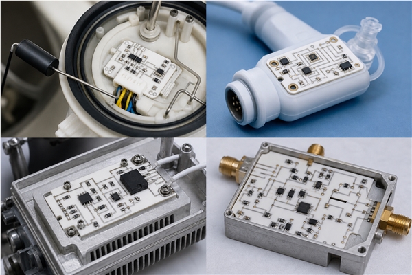
Thick film circuits are common where ceramic stability and an integrated passive function provide a real benefit:
- Automotive fuel-level, pressure, exhaust, and position sensors
- Medical sensor interfaces and compact diagnostic electronics
- Industrial heaters, temperature controllers, and high-temperature instrumentation
- Power resistor networks, current sensing, and discharge circuits
- Hybrid microelectronics with bare die, wire bonds, or compact passive networks
- Communications modules that need ceramic stability without the finest thin-film geometry
Current BST examples include a thick film ceramic substrate for an automotive oil-level sensor, an Al2O3 thick film substrate for medical equipment, and a gold-conductor thick film substrate for communication electronics. These examples show application fit; the final paste system and geometry still require design-specific qualification.
What Causes Thick Film PCB Defects?
| Problem | Likely cause | Prevention |
|---|---|---|
| Open or narrowed conductor | Blocked screen, poor paste transfer, contamination, or excessive edge loss | Control screen condition, print setup, paste handling, and minimum neck width |
| Smearing or bleeding | Incorrect viscosity, excessive squeegee pressure, poor snap-off, or insufficient drying | Lock the print window and verify wet and fired geometry |
| Poor adhesion | Dirty ceramic, incompatible paste, wrong firing profile, or too many thermal cycles | Qualify surface preparation and the complete material stack |
| Resistor value drift | Geometry variation, refiring, substrate interaction, trim damage, or excess power density | Use process coupons, planned firing order, controlled trim, and thermal derating |
| Dielectric pinholes or leakage | Contamination, trapped gas, thin print, or registration error | Use qualified dielectric thickness, overlap, inspection, and isolation testing |
| Solder leaching or poor bondability | Conductor chemistry does not match the assembly process | Select a termination system for the actual solder, dwell time, wire, and temperature |
| Ceramic cracks | Edge defects, mounting stress, local hot spots, or CTE mismatch | Control machining, support, attachment area, thermal gradients, and assembly pressure |
When Should You Choose a Thick Film PCB?
Choose thick film when the design benefits from at least one native thick-film function: printed resistors, a heater pattern, a compact ceramic hybrid, high-temperature operation, stable sensing geometry, or a paste-based conductor system. It is also attractive when production volume can justify screens and process qualification while avoiding many discrete passive components.
Do not choose it only because “ceramic dissipates heat.” Use thin film when precision and fine RF geometry dominate. Use DBC or AMB when high current and thick copper are central. Use DPC when plated copper and finer ceramic routing are required. Use FR4 when the circuit is a conventional multilayer assembly and its temperature, insulation, and thermal path are already adequate.
What Are the Most Common Thick Film PCB Questions?
Is a thick film PCB the same as a thick copper PCB?
No. Thick film refers to printed and fired functional paste. Thick copper refers to a comparatively thick copper conductor layer formed by foil bonding, etching, or plating.
What is the most common thick film PCB substrate?
96% alumina is the common workhorse because it balances electrical insulation, process compatibility, mechanical stability, availability, and cost.
How thick is a fired thick film conductor?
A single fired print is often around 10-20 micrometers, but actual thickness varies with paste, mesh, emulsion, printing conditions, and firing shrinkage. Some systems use multiple prints or etchable pastes.
What temperature is used to fire thick film paste?
Many conventional air-fired conductor and resistor systems use a peak near 850°C. Low-temperature and specialized systems use other profiles, so the paste data sheet and substrate qualification control the real process.
Can resistors be printed directly on the ceramic?
Yes. Printed resistor pastes can form individual resistors or matched networks. Their geometry and sheet resistance establish the nominal value, and laser trimming can adjust selected values after firing.
Can a thick film PCB use aluminum nitride?
Yes, but the AlN grade, surface condition, paste chemistry, atmosphere, and firing profile must be compatible. An alumina process should not be transferred to AlN without qualification.
Can thick film ceramic PCBs have vias?
They can, provided the hole geometry, via-fill paste, print method, firing sequence, and connection to surface conductors are designed as one process. A drilled hole alone is not a conductive via.
Is thick film suitable for RF circuits?
It can support some RF and microwave functions, especially where moderate geometry is acceptable. Thin film is usually preferred when very fine lines, tight impedance control, low loss, or highly repeatable precision dominates.
Can components be soldered or wire bonded to thick film conductors?
Yes, when the conductor paste and any surface finish are designed for that attachment method. Solderability, solder leach resistance, gold or aluminum wire compatibility, and thermal exposure must be specified.
How do you choose between thick film and DBC?
Choose thick film for printed resistors, heaters, functional pastes, and compact hybrid integration. Choose DBC when thick copper, high current, and strong lateral heat spreading are the primary requirements.
What Is the Practical Takeaway?
A thick film pcb is a strong choice when printed functional layers and ceramic stability solve a specific electrical, thermal, or packaging problem. The decision should be based on the complete substrate-paste-firing-assembly system, not on ceramic material alone. For a design review focused on material compatibility, layer sequence, printed resistors, pads, vias, or production tests, contact BSTCeramicPCB at sales@bstceramicpcb.com.
 Products
 About us
 Contact us



