






















































 HOME


-

Ceramic PCB for Humanoid Robot joint actuators
2026 04,07 -
LTCC PCB Surprises: What Most People Miss
2025 12,09 -
Step-by-Step Guide to DPC PCB Design for Sensor Systems
2025 12,03 -
Ceramic PCBs Essential Benefits and Applications
2025 12,01 -
How Al2O3 DPC Ceramic Substrate PCB Enhances Heat Dissipation in Modern Electronics?
2025 11,28 -
How to Choose Between Ceramic, FR4, and Metal Core PCBs
2025 11,27 -
DPC Ceramic PCB Materials: Surprising Science Inside
2025 11,26 -
Wire bondable 2-layer Alumina substrates PCB | Bstceramic PCB
2025 09,22 -
Silicon Nitride Substrate, Silicon Nitride Ceramic Substrate Formula
2025 05,08 -
What is thick film ceramic PCB?
2023 08,02
How Does Thick Film Screen Printing Build Ceramic PCB Circuits?
Published:
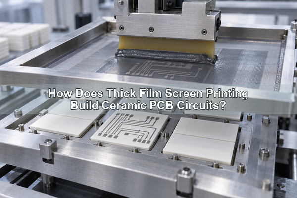
Thick Film Screen Printing transfers functional paste through a patterned mesh onto a ceramic substrate. The print is then dried and fired so the deposited material becomes a conductor, resistor, dielectric or protective layer. In ceramic PCB production, the result depends on the complete material and process system: substrate condition, paste rheology, screen geometry, squeegee settings, registration, drying and firing must work together.
What Is Thick Film Screen Printing?
Thick film screen printing is an additive patterning process for functional electronic materials. A squeegee moves paste across a screen. Paste passes through the open image areas and remains on the ceramic in the required circuit pattern. The process can create conductive traces, resistor elements, dielectric insulation, crossovers and selected protective features.
The term describes the deposited electronic film, not the thickness of the ceramic board. It should also not be confused with textile high-density printing or a thick-copper PCB.
How Does Thick Film Screen Printing Work on Ceramic?
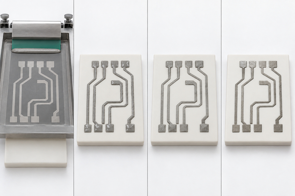
A typical fired-ceramic process follows a controlled print-dry-fire sequence:
- Clean and fixture the ceramic substrate so its surface is dry, uncontaminated and stable.
- Align the patterned screen to the substrate fiducials or tooling features.
- Flood the screen with paste, then move the squeegee across the image under controlled speed and pressure.
- Allow the paste to level, inspect the wet print and dry it according to the paste system.
- Fire the dried layer on its qualified thermal profile to remove organics and develop adhesion and electrical properties.
- Repeat compatible print, dry and fire cycles when the design needs resistors, dielectric layers, crossovers or overglaze.
Which Ceramic Substrates and Pastes Are Used?
The substrate and paste must be selected as a compatible system. Alumina is widely used for fired thick-film circuits because it provides electrical insulation, dimensional stability and established conductor, resistor and dielectric paste options. Aluminum nitride may be selected when a higher-conductivity ceramic is required, but its surface preparation and paste compatibility need process review.
| Material input | Function in the circuit | What the engineering team should specify |
|---|---|---|
| Ceramic substrate | Mechanical support, electrical insulation and thermal path | Material grade, thickness, flatness, surface condition and finished outline |
| Conductor paste | Traces, pads, electrodes and terminations | Assembly method, current path, soldering or wire-bonding needs and target fired thickness |
| Resistor paste | Printed resistance element | Target resistance, tolerance, power loading, geometry and trimming requirement |
| Dielectric paste | Insulation, crossovers and multilayer separation | Voltage stress, overlap, fired thickness and compatibility with adjacent layers |
| Overglaze or protective paste | Environmental or mechanical protection | Open-pad areas, operating environment and later assembly steps |
Paste chemistry is not interchangeable. A fired ceramic paste typically contains a functional phase, an inorganic bonding phase and an organic vehicle that provides printable flow. Its datasheet governs storage, mixing, drying and firing conditions.
How Do the Screen, Mesh, Emulsion and Artwork Affect the Print?
The screen determines where paste can pass and strongly influences deposited volume and edge definition. Mesh count, wire diameter, mesh tension, emulsion thickness and image quality must be selected together with paste particle size and target geometry.
A thicker stencil opening can increase wet deposit, but it may also make fine release and edge control harder. Low or uneven screen tension can distort the image during the squeegee stroke. Poorly prepared artwork or insufficient fiducial strategy may print acceptably on a single layer yet fail when a dielectric or second conductor must register to it.
Which Printing Parameters Control Line Quality?
The practical process window is a combination, not one machine setting. The most influential controls usually include:
- Squeegee speed: affects paste transfer, shear and the time available for the mesh to release.
- Squeegee pressure: must clear the image without excessive screen deflection or paste smearing.
- Squeegee hardness and edge condition: influence deformation, print thickness and edge definition.
- Snap-off or peel behavior: controls how the screen separates from the wet print.
- Flood conditions: affect how consistently the openings refill before each print.
- Paste temperature and rheology: change flow, leveling and release as the production run progresses.
- Substrate support and registration: prevent movement, tilt and layer-to-layer offset.
Changing one parameter can move several results at once. For example, extra pressure may appear to improve incomplete transfer while increasing image distortion and line width. A stable process window should be established on the actual paste, screen, substrate and circuit pattern.
How Do Drying and Firing Change the Printed Layer?
The wet print is not the final conductor. Drying removes much of the volatile vehicle and stabilizes the layer for handling. Firing removes remaining organics and develops bonding, densification and the intended electrical behavior. The fired film is therefore thinner and materially different from the wet deposit.
Ramp rate, peak temperature, time at temperature, furnace atmosphere and cooling profile must follow the qualified material system. An incorrect profile can leave carbon residue, create poor adhesion, change resistance, blister a dielectric or damage an earlier layer. Repeated firing also exposes previous prints to additional thermal history, so the sequence of conductor, dielectric, resistor and overglaze layers matters.
What Can Be Printed in a Thick-Film Ceramic Circuit?
Screen printing can integrate more than copper-like interconnects. Depending on the qualified paste system, a ceramic circuit may combine:
- conductor traces and solder pads;
- printed resistors that are measured and laser trimmed;
- dielectric insulation and crossover structures;
- heater tracks, sensor electrodes or potentiometer paths;
- surface protection with defined openings for attachment and test.
Our Al2O3 thick-film circuit for medical devices uses a two-layer 96% alumina construction with 10-15 micrometer AgPd conductors. It is a useful example of why the required function, paste system and layer sequence should be specified together rather than treating every printed ceramic as the same board.
How Is Thick Film Screen Printing Different from SMT Stencil Printing?
Both processes push paste through patterned openings, but their outputs and downstream operations are different.
| Decision point | Thick-film ceramic screen printing | SMT solder-paste stencil printing |
|---|---|---|
| Deposited material | Functional conductor, resistor or dielectric paste | Solder paste for component attachment |
| Substrate | Commonly a ceramic circuit substrate | A fabricated PCB with component pads |
| Main purpose | Create part of the circuit itself | Prepare joints before component placement |
| Thermal step | Qualified drying and firing or curing process | Reflow soldering after placement |
| Key result | Fired electrical, resistive or insulating layer | Solder-joint volume and assembly quality |
Design data for one process cannot be copied directly to the other. A solder-paste aperture rule does not define a fired thick-film line, and a thick-film conductor print does not replace assembly stencil engineering.
When Should You Choose Thick Film Instead of Thin Film or DPC?
Choose the process from the required geometry, metal system, integrated functions and production economics.
| Requirement | Thick film | Thin film | DPC |
|---|---|---|---|
| Printed resistors or heaters | Strong fit | Possible with a different deposition stack | Usually not the main reason to choose it |
| Fine conductor geometry | Moderate, process-dependent | Strong fit for fine features | Strong fit for patterned copper features |
| Conductor build | Printed and fired paste | Deposited metal film | Plated copper |
| Tooling economics | Screen cost can suit repeat production | Higher process complexity | Photolithography and plating route |
| Best selection question | Do printed functional materials add value? | Is fine geometry or controlled thin metal essential? | Is plated copper thickness and geometry the priority? |
Thick film is unnecessary when a standard organic PCB meets the temperature, insulation, geometry and reliability needs. It is also a weak choice when the design requires line definitions beyond the qualified screen-printing capability and has no need for printed functional layers.
What Are the Most Common Screen-Printing Defects?
Defects should be traced to the print system rather than corrected by changing one setting blindly.
| Defect | Likely process contributors | Engineering response |
|---|---|---|
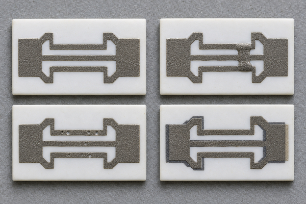
| Incomplete or broken line | Blocked opening, poor paste release, low deposit or contaminated substrate | Inspect screen, paste condition, wet print and substrate cleanliness |
| Bridging or smeared edge | Excess pressure, damaged squeegee, low screen tension or unsuitable rheology | Restore screen and squeegee condition; re-establish the print window |
| Pinholes or voids | Air, contamination, poor leveling or firing-related outgassing | Review paste handling, surface condition, drying and thermal profile |
| Layer misregistration | Fixture movement, artwork error, screen stretch or weak fiducial plan | Verify tooling, registration method and layer-stack tolerances |
| Variable fired resistance | Geometry variation, thickness variation, paste lot or firing variation | Correlate print measurements, firing records and post-fire resistance |
| Blistering or delamination | Trapped solvent, incompatible layers or incorrect firing | Check drying completeness, compatibility and thermal sequence |
How Should a Ceramic PCB Be Designed for Repeatable Printing?
Repeatability starts in the layout. Avoid treating the nominal artwork dimension as the guaranteed fired feature. Printed line width, spacing and thickness vary with the screen, paste and firing system, while layer-to-layer registration adds another tolerance.
At BSTCeramicPCB, our published thick-film capability table lists 125/150 micrometers as the minimum line width/space and 7-20 micrometers for conductor thickness. These are capability references, not automatic acceptance criteria for every material stack. Narrow conductors, large print areas, mixed pastes, multiple firings and critical resistor geometries require an engineering review against the actual design.
Use clear fiducials, adequate dielectric overlap, realistic edge clearance and test access. Tell the manufacturer which dimensions are electrically or mechanically critical instead of applying the tightest tolerance to every feature.
How Are Printed Ceramic Circuits Inspected and Qualified?
Inspection should follow the risks created by the design. Visual or automated optical inspection can find contamination, incomplete print, bridging and registration errors. Dimensional measurement verifies critical lines, pads and overlaps. Electrical tests confirm continuity, isolation and resistance after firing.
Qualification may also require adhesion, solderability, wire-bond evaluation, thermal cycling or environmental testing. The required test plan depends on the paste system, assembly interface and end-use standard. A print that looks clean is not enough if its fired resistance, adhesion or insulation fails the functional requirement.
What Project Data Is Needed for Manufacturing Review?
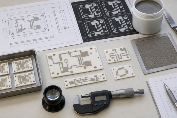
A complete project package lets the manufacturer evaluate the material stack and process window before screen tooling is released. Provide:
- Gerber, ODB++, DXF or another agreed pattern file, plus a dimensioned drawing;
- ceramic material, grade, thickness, outline and flatness requirements;
- conductor, resistor, dielectric and overglaze functions;
- target fired thickness and critical line, space, pad and overlap dimensions;
- resistance values, tolerances, power loading and trimming requirements;
- soldering, brazing, wire-bonding, conductive-epoxy or other attachment method;
- operating temperature, voltage, environment and applicable qualification standard;
- prototype quantity, production forecast, panel preference and required test records.
For example, our AgPd and gold thick-film communication substrate combines a two-layer 96% alumina board with 10-15 micrometer AgPd and a 5 micrometer gold layer. Our automotive oil-level sensor ceramic circuit uses a different one-layer AgPd construction with green glass glaze. These examples show why the drawing must identify both the electrical function and the surface or assembly requirement.
FAQ
How thick is a screen-printed thick film?
There is no universal value. The fired thickness depends on paste chemistry, mesh, emulsion, print settings, leveling and firing. Specify a target or acceptable range and verify it with the selected paste system rather than using wet-print thickness as the final value.
Can multiple thick-film layers be screen printed?
Yes. Compatible conductor and dielectric layers can be printed in sequence, with controlled drying and firing between operations. Registration, dielectric overlap and accumulated thermal history become more important as the stack grows.
Can thick film screen printing make fine lines?
It can produce relatively fine patterns, but the practical limit depends on the complete screen, paste and substrate process. When geometry is beyond the qualified printing window, thin film, DPC or a photo-definable thick-film process may be more suitable.
Are all thick-film pastes fired at the same temperature?
No. Conductor, resistor, dielectric and polymer systems have different profiles and atmospheres. Use the selected material supplier's datasheet and the manufacturer's qualified process; do not combine pastes only because their product names sound similar.
Does screen printing replace laser trimming?
No. Printing establishes the resistor geometry and material. Laser trimming is a later adjustment step used when a design needs a tighter final resistance than printing and firing alone can reliably provide.
From Prototype to Production
Thick Film Screen Printing is most effective when circuit geometry, paste selection, screen design, thermal processing and assembly are reviewed as one manufacturing system. A prototype should verify fired dimensions, electrical performance, adhesion and the intended attachment process before tooling and test limits are frozen for production.
BSTCeramicPCB can review your ceramic material, printed functions, critical tolerances and qualification requirements before quotation. Send the drawing, stack information and expected quantity to sales@bstceramicpcb.com.
 Products
 About us
 Contact us



