






















































 HOME


-

Wire Bonding EPIG Thickness: Selecting Pd/Au for Ceramic Bond Pads
2026 10,19 -
When Does a Thin-Film Circuit Need a Polished Alumina Substrate?
2026 10,18 -
Ceramic PCB for Humanoid Robot joint actuators
2026 04,07 -
LTCC PCB Surprises: What Most People Miss
2025 12,09 -
Step-by-Step Guide to DPC PCB Design for Sensor Systems
2025 12,03 -
Ceramic PCBs Essential Benefits and Applications
2025 12,01 -
How Al2O3 DPC Ceramic Substrate PCB Enhances Heat Dissipation in Modern Electronics?
2025 11,28 -
How to Choose Between Ceramic, FR4, and Metal Core PCBs
2025 11,27 -
DPC Ceramic PCB Materials: Surprising Science Inside
2025 11,26 -
Wire bondable 2-layer Alumina substrates PCB | Bstceramic PCB
2025 09,22 -
Silicon Nitride Substrate, Silicon Nitride Ceramic Substrate Formula
2025 05,08 -
What is thick film ceramic PCB?
2023 08,02
Wire Bonding EPIG Thickness: Selecting Pd/Au for Ceramic Bond Pads
Published:
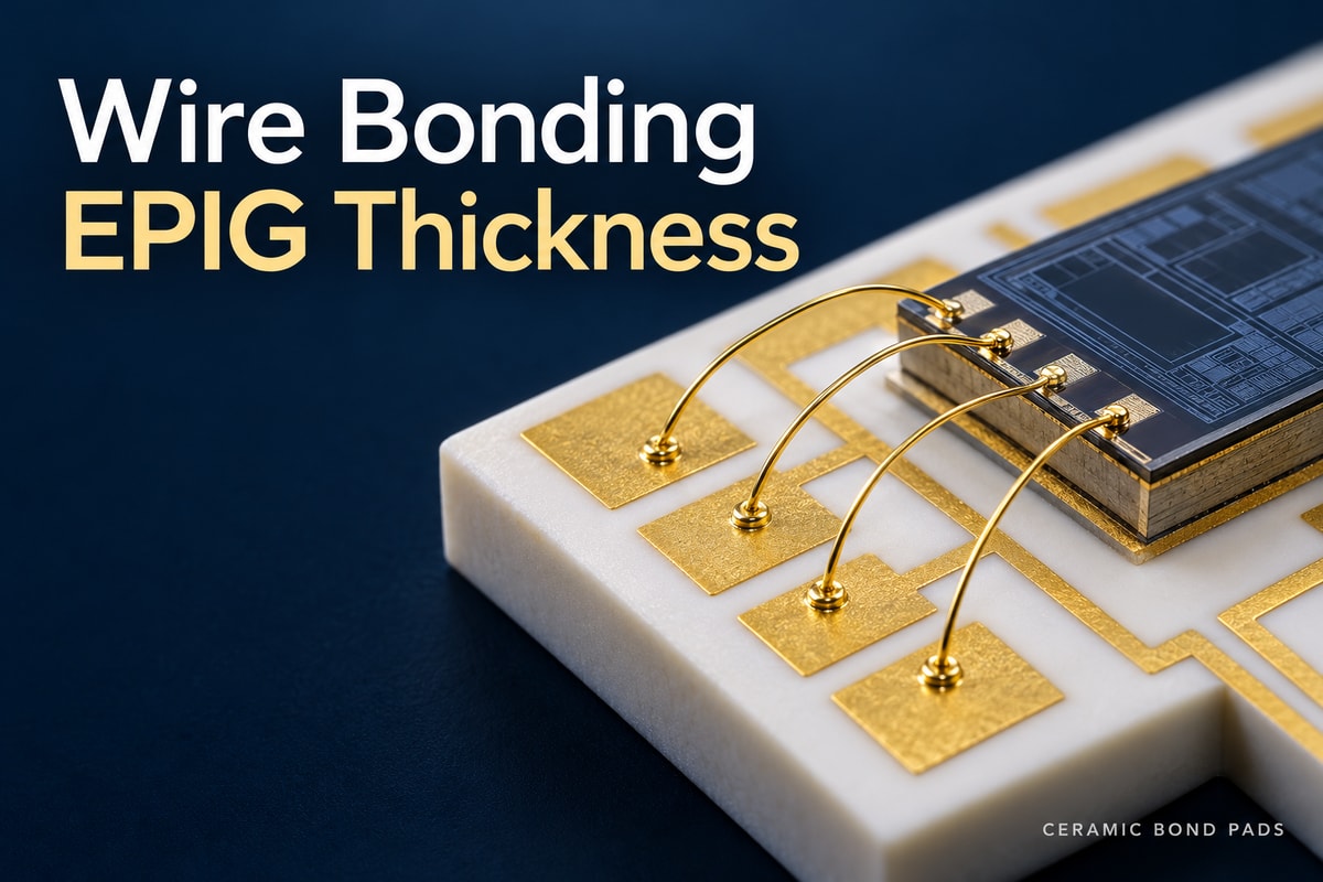
Choosing wire bonding EPIG thickness starts with two separate numbers: palladium thickness and gold thickness. This guide explains how to assess a proposed combination, decide whether thermal exposure changes your requirements, and identify the evidence needed before using that finish on ceramic bond pads.
BSTCeramicPCB supports your ceramic PCB project from design review through prototyping and production. Our engineers review your pad metallization, requested Pd/Au thicknesses, and assembly requirements to identify specification gaps and assess process compatibility before fabrication. With DFM pre-review and sample and small-batch manufacturing support, you can evaluate your design before committing to a larger production order. Planning a ceramic PCB prototype? Send your drawings and wire-bonding requirements to sales@bstceramicpcb.com for an engineering review and quotation. Our team will help clarify your specifications and assess the manufacturing options for your project.
What Wire Bonding EPIG Thickness Should You Specify for Ceramic PCBs?
Use a Pd/Au combination qualified for your pad stack and bonding process, with separate acceptance limits for each layer. If no qualified specification exists, select a trial combination with the finishing supplier before setting production limits.
A published reference worth discussing is 0.20 µm Pd plus 0.20 µm Au. This target combination has been reported under the conditions below; it is a supplier example, not a universal ceramic-board minimum.
| Parameter | Published reference |
|---|---|
| Pd target | 0.20 µm ≈ 7.9 µin |
| Au target | 0.20 µm ≈ 7.9 µin |
| Wire | Gold, 25.4 µm diameter |
| Heat exposure before bonding | 175°C for 16 hours |
| Assessment | Wire pull strength and failure mode |
This example is not a BSTCeramicPCB capability specification or evidence that your ceramic construction is qualified.
How should you use that information?
- Existing qualified design: Keep its approved layer limits unless a material or process change requires requalification.
- New copper-metallized design using gold wire: Ask whether the supplier has supporting data for a comparable Pd/Au stack, wire diameter, and thermal sequence. Use that evidence to select samples.
- Different metallization or wire: Request evidence for that combination. Matching the ceramic material alone is insufficient.
A drawing that says “EPIG 0.4 µm” is incomplete: it does not distinguish 0.2/0.2 µm from 0.1/0.3 µm. Even “Pd 0.2 µm / Au 0.2 µm” needs clarification: are these targets or minimums? Specify the meaning, accepted limits, and measurement locations before ordering.
Why Do EPIG and ENEPIG Plating Need Different Thickness Specifications?
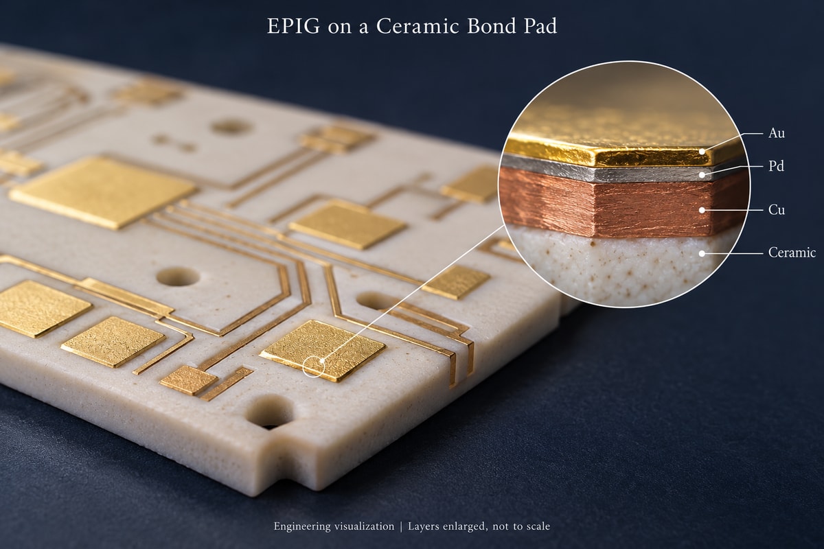
Because removing nickel changes both the layer beneath the palladium and the finished metallization build-up. Keeping the same Pd/Au values does not preserve the original ENEPIG structure.
| What changes? | EPIG | ENEPIG |
|---|---|---|
| Copper-pad stack | Cu / Pd / Au | Cu / Ni / Pd / Au |
| Metal beneath Pd | Copper | Nickel |
| Layers requiring limits | Pd, Au | Ni, Pd, Au |
| Build-up to assess | Pd + Au | Ni + Pd + Au |
When converting an ENEPIG drawing to EPIG, check two things:
- Bond qualification: Was the evidence obtained on copper/Pd/Au or nickel/Pd/Au? An unchanged gold thickness does not make those results interchangeable.
- Finished geometry: Check pad dimensions, spacing, and any height-sensitive assembly features against the new build-up.
Also distinguish “nickel-free finish” from “nickel-free pad stack.” If the underlying ceramic metallization already contains nickel, specifying EPIG at the surface does not remove that buried layer.
For a ceramic board, write out the complete metal stack. That makes a proposed finish substitution visible to both the fabricator and the bonding team.
How Should You Balance Palladium and Gold Thickness?
Evaluate palladium for its barrier performance after heating and gold for the bondable surface it provides. Choose the combination that meets your post-process bond criteria; do not optimize either thickness in isolation.
A published study on copper-clad laminate coupons illustrates why. As-plated EPIG pull results improved with thicker gold, while palladium thickness showed little influence. After 175°C for 16 hours, thinner palladium performed worse; thicker gold also helped. Surface analysis linked these effects to copper diffusion and palladium enrichment at the gold surface. These results were obtained with gold wire on test coupons, not ceramic production boards.
Turn that distinction into a controlled comparison. Ask your suppliers to select two manufacturable Pd levels and two Au levels, then compare:
| Trial | Pd level | Au level | Comparison purpose |
|---|---|---|---|
| A | Lower | Lower | Establish the baseline |
| B | Higher | Lower | Isolate the Pd change |
| C | Lower | Higher | Isolate the Au change |
| D | Higher | Higher | Check their combined effect |
This is a proposed screening method, not a published set of recommended thicknesses. Keep pad construction, wire, bonding settings, and thermal exposure consistent across the trials.
- If B improves post-heat results over A: The Pd change deserves further evaluation. Confirm repeatability and failure locations before attributing the improvement to a barrier mechanism.
- If C improves results over A: The Au change is useful under those conditions. Check whether the improvement survives the full thermal sequence.
- If only D passes: Verify the combined stack; neither single-layer change has demonstrated an adequate solution.
- If all trials fail similarly: Investigate cleanliness, bonding settings, and pad integrity before paying for still thicker coatings.
Once several combinations pass, compare their result spread, production capability, and cost. A single high pull value is not a sound basis for selecting the cheapest or thickest finish.
Will the Bonding Surface Remain Reliable After Thermal Processing?
You can accept it for the tested process only when samples exposed to the planned thermal sequence still meet the agreed strength and failure-mode criteria. An as-received pass cannot answer that question.
Use samples from the same finish lot to make three comparisons:
- As received → bond → test: Establish the starting result.
- Planned pre-bond heating → bond → test: Determine whether baking or curing reduces subsequent bondability.
- Bond → planned downstream heating → test: Determine whether already-formed bonds survive later processing.
Include the actual bake duration and number of thermal exposures. The reference 175°C/16-hour condition is not a substitute for your own sequence.
Interpret the result before changing thickness. If only preheated pads perform poorly, focus the investigation on surface changes and the pre-bond process. If only completed, heat-exposed bonds deteriorate, investigate the bonded interface and downstream sequence. If all groups perform poorly, thermal exposure alone does not explain the problem.
Apply acceptance limits to individual results and allowed failure modes, not just the group average. A satisfactory mean can hide weak bonds that need investigation.
How Do Wire Material and Bonding Method Affect EPIG Selection?
They determine which qualification data are transferable and which tests your samples need. Gold-wire evidence supports a gold-wire comparison; it does not automatically qualify aluminum, copper, or palladium-coated copper wire.
Use these checks when your assembly plan changes:
- Different wire alloy or coating: Request bond and aging results for that wire-to-finish combination. Do not assume changing Au thickness will compensate for a different interface.
- Different wire diameter: Revisit the bond footprint, pad clearance, and strength criteria. A force limit developed for one diameter should not be copied without justification.
- Ball-to-wedge process change: Confirm tool access, bond footprint, and support on the actual ceramic part. The coating can remain unchanged while the mechanical requirements change.
For ball bonding, identify where the ball and second bond land. If the ceramic pad receives the second bond, a ball-shear result from the die does not demonstrate the strength of that ceramic connection.
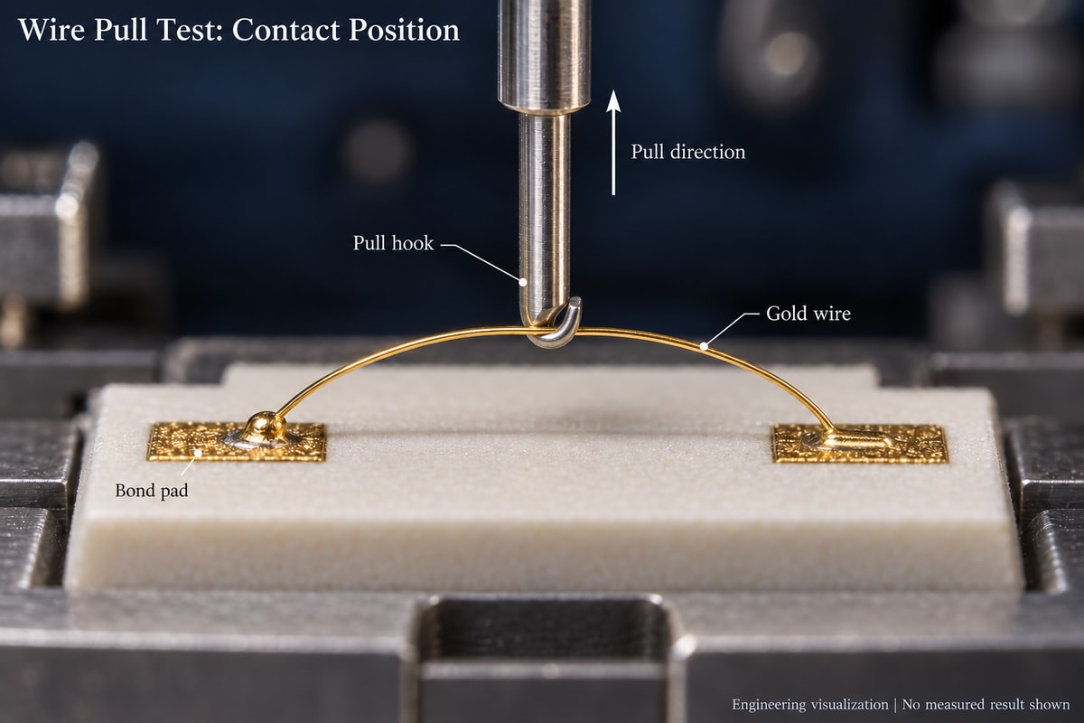
Match the test to the joint: wire pull evaluates the wire connection, while ball shear can provide additional information about a ball-to-pad interface.
How Can You Verify EPIG Thickness and Bond Quality Before Production?
Require a thickness report tied to the tested lot and bond-test results tied to the actual assembly conditions. Review both before approving production.
For the thickness report, check separate Pd/Au readings, pad locations, accepted limits, and measurement method. If XRF is used, the supplier should confirm that its calibration and measurement spot are suitable for the layer stack and pad size. A large witness coupon should not silently replace measurements representative of small bond pads.
For the bond report, ask for sample count, individual results, wire details, thermal history, and failure locations. Pull force alone can conceal which part of the connection is weak; failure mode helps identify that weakest element.
Use the observations to direct investigation:
| Observation | What to investigate next |
|---|---|
| Bond separates at pad surface | Surface condition and bonding process |
| Pad metallization detaches | Metallization adhesion and applied loading |
| Wire breaks near heel or neck | Wire deformation and bonding/loop settings |
| Wire breaks in its span | Force criterion and test geometry |
These are investigation directions, not diagnoses. A wire break does not automatically mean a pass, and a lifted bond does not prove insufficient gold thickness.
Release the design when both layers meet their limits and representative bonds meet the agreed criteria after the required exposures. If results conflict, resolve the discrepancy before approving the lot. Record the accepted stack and process revision so later substitutions can be reviewed against the same baseline.
Why Choose BSTCeramicPCB for Your Ceramic Wire-Bonding Project?
Choose BSTCeramicPCB when you need engineering support to turn a finish request into a manufacturable ceramic-board specification, with samples available before a larger production commitment.
Resolve drawing gaps through DFM review. Our DFM pre-review and process compatibility advice help identify issues such as an unspecified underlying metal stack or a thickness value without a clear target/minimum definition. R&D and PCB/PCBA engineers with 20 years of experience support these discussions.
Keep technical decisions connected. A dedicated sales contact coordinates with a three-engineer technical team. You can discuss pad construction, finish requirements, and assembly constraints through one coordinated project interface.
Evaluate samples before scaling. Our sample and small-batch support allows you to obtain boards for your agreed qualification plan before committing to higher volumes. The specific EPIG route, achievable limits, and test responsibilities must be confirmed during project review.
Bring downstream assembly into the discussion. BSTCeramicPCB integrates PCB manufacturing, component sourcing, and PCBA assembly and testing services. Sharing the planned bake, cure, and assembly sequence early helps the team review the board against its intended use. Specialized wire-bonding services and tests are confirmed separately for the project.
FAQs about Wire Bonding EPIG Thickness
1. Is 0.20 µm Pd plus 0.20 µm Au enough for my ceramic board?
It is a published reference combination, not an automatic approval. Ask for evidence matching your pad stack, wire, and thermal sequence. If that evidence is unavailable, use samples to establish accepted layer limits before production.
2. Can I specify only the total EPIG thickness?
No. A total of 0.4 µm could describe 0.2/0.2 µm or 0.1/0.3 µm Pd/Au. Specify each layer separately and state whether its value is a target, minimum, or accepted range.
3. Should I increase gold thickness when pull strength is low?
First identify the failure location and whether heating caused the decline. If the pad metallization lifts, increasing gold does not address the underlying adhesion question. Compare controlled Pd/Au changes only after checking the relevant surface and bonding conditions.
4. Can I replace ENEPIG with EPIG without another bonding trial?
Do not treat it as a like-for-like replacement. Removing nickel changes the stack. Review the finish with the assembly team and establish what requalification is needed for the intended wire and thermal sequence.
5. Can EPIG be deposited directly on bare alumina or aluminum nitride?
The copper/Pd/Au process discussed here starts from a metal surface, not bare ceramic. Provide the ceramic metallization specification so the supplier can assess process compatibility.
6. Is a passing average pull strength enough to approve samples?
No. Review individual results, sampling, and failure modes against the agreed criteria. A strong average can coexist with low-strength bonds or unacceptable interface failures.
7. What should I send BSTCeramicPCB if my thickness requirement is not finalized?
Send the ceramic drawing, complete pad stack, proposed wire and bonding method, thermal sequence, and sample quantity. Mark Pd/Au limits as pending engineering confirmation rather than inserting an unsupported production value.
Ready to start your ceramic PCB project with BSTCeramicPCB? Send your drawings, assembly requirements, and target quantities to sales@bstceramicpcb.com to request a project review and quotation. With DFM pre-review, dedicated engineering support, and sample-to-small-batch manufacturing services, we help you move from design to prototype validation and production. Want to see our manufacturing operations firsthand? Contact us to arrange a factory visit and discuss your ceramic PCB project with our team.
 Products
 About us
 Contact us



