






















































 HOME
HOME


-

Ceramic PCB for Humanoid Robot joint actuators
2026 04,07 -
LTCC PCB Surprises: What Most People Miss
2025 12,09 -
Step-by-Step Guide to DPC PCB Design for Sensor Systems
2025 12,03 -
Ceramic PCBs Essential Benefits and Applications
2025 12,01 -
How Al2O3 DPC Ceramic Substrate PCB Enhances Heat Dissipation in Modern Electronics?
2025 11,28 -
How to Choose Between Ceramic, FR4, and Metal Core PCBs
2025 11,27 -
DPC Ceramic PCB Materials: Surprising Science Inside
2025 11,26 -
Wire bondable 2-layer Alumina substrates PCB | Bstceramic PCB
2025 09,22 -
Silicon Nitride Substrate, Silicon Nitride Ceramic Substrate Formula
2025 05,08 -
What is thick film ceramic PCB?
2023 08,02
Al2O3 Aluminum Oxide for Ceramic PCBs: Grade and Process Selection
Published:
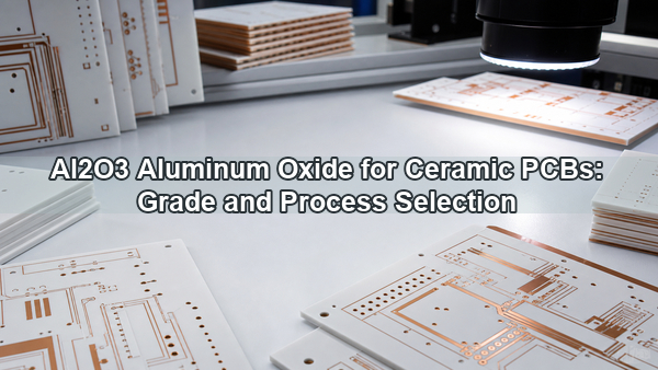
Al2O3 aluminum oxide, also called alumina, is an electrically insulating technical ceramic used as the base of thick-film, thin-film, DPC, and DBC circuit substrates. Its practical value comes from a useful combination of heat transfer, dielectric strength, dimensional stability, mechanical hardness, mature processing, and lower material cost than many high-performance ceramic alternatives. Selecting it correctly requires more than checking one thermal-conductivity value: purity, substrate thickness, metallization, copper geometry, surface condition, and assembly stresses must be evaluated together.
What Is Al2O3 Aluminum Oxide?
Al2O3 is the chemical formula for aluminum oxide, while alumina is the common engineering name for dense, sintered aluminum oxide ceramic. The ceramic is produced from refined powder with controlled additives, forming, and high-temperature sintering. PCB-grade alumina is therefore different from aluminum metal, anodized aluminum, loose abrasive powder, and aluminum-core PCB material.
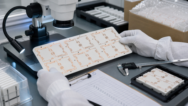
In a ceramic circuit board, the Al2O3 body provides electrical isolation and mechanical support. Conductive features are added by printing, plating, sputtering, or bonding metal onto the ceramic. The finished board may be called an alumina PCB, Al2O3 ceramic PCB, metallized alumina substrate, thick-film circuit, DPC substrate, or DBC alumina substrate, depending on how the conductor is formed.
Which Al2O3 Properties Matter for Ceramic PCBs?
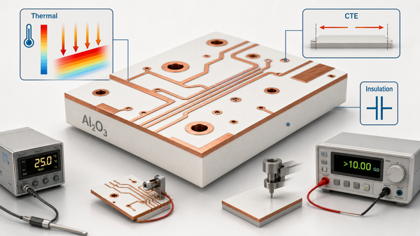
The properties that matter most are thermal conductivity, dielectric behavior, coefficient of thermal expansion, strength, surface quality, and substrate thickness. Published values vary with purity, additives, density, test method, and temperature, so production decisions should use the selected supplier's datasheet rather than a generic internet value.
| Property | Common reference for electronics-grade alumina | PCB design impact |
|---|---|---|
| Thermal conductivity | Approximately 20-30 W/m·K | Controls through-substrate heat transfer; actual board thermal resistance also depends on thickness and interfaces. |
| CTE | Approximately 6.5-8.5 ppm/K | Affects stress in copper, solder joints, die attach, and mounted components during thermal cycling. |
| Dielectric strength | Often 10-15 kV/mm or higher | Supports compact electrical isolation, subject to thickness, surface condition, contamination, and creepage design. |
| Dielectric constant | Typically about 9-10 at 1 MHz | Must be included in RF and impedance calculations; frequency-specific supplier data is required. |
| Flexural strength | Commonly about 300-500 MPa | Influences panel handling, singulation, mounting, and resistance to bending loads. |
| Water absorption | Very low for dense, fired material | Helps maintain insulation stability in humid service, but surfaces and metallization still require protection where needed. |
A thinner substrate lowers the ceramic portion of the thermal path but becomes more sensitive to handling, flatness, copper imbalance, and assembly fixtures. A thicker substrate improves rigidity and voltage spacing through the ceramic, but it increases thermal resistance. The selection should be based on the full stack, not thermal conductivity alone.
Is Al2O3 Electrically Conductive?
Al2O3 is an electrical insulator, although it conducts heat far better than common organic PCB laminates. This distinction explains its usefulness in power electronics: copper traces can remain electrically isolated while heat passes through the ceramic toward a baseplate or heat sink.
The ceramic does not replace copper. Current still flows through a printed, plated, sputtered, or bonded metal layer. Insulation performance can be reduced by surface contamination, porosity, cracks, metallization residues, insufficient edge clearance, or conductive deposits. High-voltage designs should specify operating voltage, transient voltage, pollution environment, creepage, clearance, ceramic thickness, and the required test method.
For a focused explanation of thermal versus electrical behavior, see is alumina conductive.
How Do 96% and 99.6% Alumina Substrates Differ?
96% alumina is usually the practical baseline for cost-sensitive thick-film circuits and general electronic substrates, while 99.6% alumina is selected when purity, surface quality, dielectric loss, chemical stability, or thin-film processing justifies the additional cost. A higher purity percentage is not automatically better for every PCB.
| Selection factor | 96% alumina | 99.6% alumina |
|---|---|---|
| Typical positioning | Mature, economical electronic substrate | High-purity precision substrate |
| Common process fit | Thick film, many DPC and DBC designs | Thin film, sputtering, fine surface applications |
| Surface requirement | Adequate for many printed and bonded conductors | Available with finer, more consistent surface finishes |
| Electrical performance | Suitable for many industrial and power circuits | Often selected for lower loss or stricter dielectric consistency |
| Cost and availability | Lower cost and broadly available | Higher material and processing cost |
Specify 99.6% only when the application or metallization process benefits from it. If a conventional thick-film circuit meets voltage, thermal, dimensional, and reliability targets on 96% alumina, increasing purity may add cost without solving a real constraint. For a deeper grade comparison, review 96 alumina properties and substrate applications.
Which Metallization Processes Work with Al2O3?
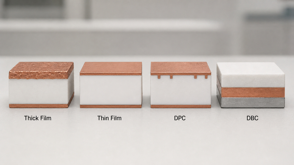
Al2O3 supports several metallization routes, but they produce different conductor thicknesses, feature sizes, adhesion mechanisms, finishes, and cost structures. The process must be selected from current density, thermal path, line/space, wire-bonding, assembly finish, and production-volume requirements.
| Process | Conductor approach | Best fit | Key review point |
|---|---|---|---|
| Thick film | Screen-printed metal paste fired onto ceramic | Hybrid circuits, sensors, resistors, moderate-current routing | Paste system, fired thickness, sheet resistance, adhesion, and overglaze compatibility |
| Thin film | Sputtered or deposited seed layers with patterned metal | Fine features, RF, photonics, precision circuits | Surface roughness, adhesion layer, line tolerance, and final finish |
| DPC | Seed layer plus plated copper | Fine-to-medium features, controlled copper thickness, thermal modules | Via structure, copper thickness distribution, plating adhesion, and warpage |
| DBC | Relatively thick copper directly bonded to ceramic | Power modules and high-current heat spreading | Copper/ceramic thickness balance, etched geometry, edge clearance, and thermal cycling |
A DBC drawing should not reuse thin-film line rules, and a thick-film quote cannot be defined by copper ounces alone. The RFQ must name the intended technology or provide electrical and mechanical requirements that allow the manufacturer to recommend one.
How Does Al2O3 Compare with FR4, AlN, and Si3N4?
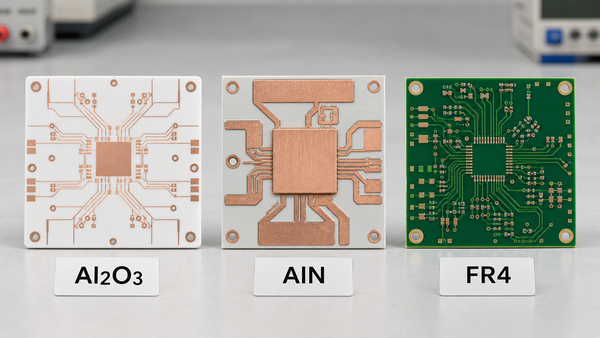
Al2O3 is normally chosen for balanced cost, insulation, temperature capability, and process maturity. FR4 remains preferable for economical multilayer signal routing; AlN is preferable when through-substrate heat transfer is the dominant constraint; Si3N4 is preferable when mechanical toughness and power-cycling reliability justify its cost.
| Material | Thermal position | Mechanical/electrical position | Use it when |
|---|---|---|---|
| FR4 | Low through-plane heat transfer | Excellent multilayer routing economy | Power density and operating temperature remain within laminate capability. |
| Al2O3 | Moderate ceramic heat transfer | Strong insulation, hardness, and mature processing | The design needs a cost-effective ceramic substrate without extreme heat flux. |
| AlN | Much higher than alumina | Electrical insulation with CTE closer to silicon | Junction temperature or heat flux cannot be controlled with a practical alumina thickness. |
| Si3N4 | High, but usually below premium AlN grades | High fracture toughness and thermal-cycle capability | Power cycling, vibration, or mechanical reliability is the primary risk. |
Do not select AlN simply because its bulk thermal conductivity is higher. Compare total thermal resistance from the device junction through die attach, copper, ceramic, interface material, baseplate, and heat sink. If the interface or heat sink dominates, a more expensive substrate may produce little system-level improvement. See the dedicated alumina vs aluminum nitride ceramic PCB comparison for additional material trade-offs.
Where Are Al2O3 Ceramic PCBs Used?
Al2O3 ceramic PCBs are used where electrical insulation, moderate heat transfer, dimensional stability, and environmental resistance are needed without the cost of AlN or Si3N4. Typical applications include:
- LED and laser-diode modules with controlled heat flow to a housing.
- Power supplies, converters, gate-driver circuits, and industrial power modules.
- Automotive sensors, control electronics, and high-temperature under-hood modules.
- Thick-film resistor networks, heaters, and precision sensor circuits.
- Medical, analytical, and industrial instruments requiring chemical stability and insulation.
- RF and microwave circuits when the selected purity, surface finish, thickness, Dk, and loss data meet the frequency requirement.
Alumina should be avoided when the circuit requires economical high-layer-count routing, flexing, large-area mechanical compliance, or heat removal beyond the capability of the complete thermal stack. Those cases may call for FR4, flex circuits, metal-core structures, AlN, or another ceramic system.
What Design Limits Need Early Review?
Ceramic brittleness, metallization thickness, panel format, and assembly stress must be reviewed before layout release. The most expensive changes are often caused by treating an Al2O3 board like a standard routed FR4 PCB.
- Outline and corners: use practical radii where possible and identify laser cutting, scribing, dicing, or other singulation needs.
- Holes and slots: specify finished size, positional tolerance, plated or unplated condition, and whether the hole carries current or only provides mounting.
- Trace geometry: line/space depends strongly on thick film, thin film, DPC, or DBC processing and metal thickness.
- Copper balance: large asymmetric copper areas can increase bow and stress, especially on thin ceramic.
- Edge clearance: voltage, copper thickness, etching behavior, and mechanical singulation all affect the required distance from metal to the ceramic edge.
- Assembly load: connector insertion, screw torque, clamping, and fixture pressure can crack ceramic even when the thermal design is acceptable.
- Thermal interfaces: define die attach, solder, thermal-interface material, baseplate flatness, and heat-sink mounting.
A prototype should reproduce the intended ceramic grade, thickness, metallization, finish, and singulation method. A simplified coupon may verify conductor adhesion or dielectric behavior, but it cannot validate full-board warpage, mounting stress, or the final thermal path.
How Should Engineers Select an Al2O3 Substrate?
Select the substrate by starting with system limits and then choosing the least complex construction that satisfies them. A practical sequence is:
- Define operating and peak voltage, component power, allowable junction temperature, ambient range, and thermal-cycle profile.
- Model the complete thermal path and test at least one realistic assembly stack.
- Choose 96% or 99.6% purity from dielectric, surface, frequency, chemical, and process requirements.
- Select thick film, thin film, DPC, or DBC from current, line/space, conductor thickness, finish, and volume.
- Confirm ceramic thickness, panel format, holes, edge clearance, flatness, and singulation with the fabricator.
- Validate adhesion, insulation, thermal performance, and assembly stress on production-representative prototypes.
This approach keeps Al2O3 aluminum oxide in the design only when it provides the required performance at a defensible cost. It also makes the reason for upgrading to AlN or Si3N4 measurable rather than speculative.
What Should Buyers Include in an Al2O3 PCB RFQ?
A complete RFQ should define the substrate, circuit, finish, mechanical requirements, validation conditions, and order profile. Provide the following information:
- Gerber or ODB++ data, fabrication drawing, and a dimensioned mechanical file.
- Alumina purity and preferred material grade, or the required property limits.
- Ceramic thickness, finished dimensions, tolerance, flatness, and edge condition.
- Metallization process, conductor material, copper or film thickness, and line/space.
- Via, hole, slot, cavity, scribe-line, and singulation requirements.
- Surface finish, wire-bonding or soldering method, solder mask or passivation needs.
- Operating voltage, current, power, temperature range, heat-sink arrangement, and reliability target.
- Prototype quantity, annual demand, panel or single-piece delivery, inspection, and test requirements.
BSTCeramicPCB can review these inputs before quotation to identify missing specifications, process conflicts, and prototype validation needs. The review is most useful before the layout is frozen, especially for thin ceramic, thick copper, fine features, high voltage, or wire-bondable finishes.
FAQ About Al2O3 Aluminum Oxide
1. Is alumina the same as Al2O3?
Yes. Alumina is the common technical name for aluminum oxide, whose chemical formula is Al2O3. Commercial ceramics contain Al2O3 plus controlled additives, so the purity grade must still be specified.
2. Is Al2O3 suitable for high-power PCBs?
It is suitable when the calculated heat flux and total thermal resistance remain within the component temperature limit. DBC alumina can provide thick copper for current handling and heat spreading, but AlN may be needed when the ceramic layer is the dominant thermal bottleneck.
3. Does higher alumina purity always improve a PCB?
No. Higher purity can improve selected dielectric, surface, and chemical properties, but it may not improve a standard thick-film or DBC design enough to justify the cost. Match purity to measurable requirements.
4. Can Al2O3 ceramic be machined after sintering?
Dense fired alumina is hard and brittle, so post-sintering machining normally requires diamond tools, laser processing, or grinding. Holes, slots, and outlines should be defined early because geometry, tolerance, and edge quality affect cost and fracture risk.
5. What is the main limitation of an alumina PCB?
The main limitations are brittleness and lower thermal conductivity than AlN. It also does not provide the economical multilayer routing density of FR4, so it should be used where its ceramic properties solve a specific system constraint.
Conclusion
Al2O3 is a practical ceramic PCB substrate when a design needs electrical insulation, moderate heat transfer, dimensional stability, and mature metallization at a controlled cost. The decisive checks are purity, thickness, metallization method, total thermal resistance, copper balance, assembly stress, and validation requirements. For material or process review before quotation, contact BSTCeramicPCB at sales@bstceramicpcb.com with your circuit files, mechanical drawing, operating conditions, and expected volume.
 Products
 About us
 Contact us



