






















































 HOME
HOME


-

Ceramic PCB for Humanoid Robot joint actuators
2026 04,07 -
LTCC PCB Surprises: What Most People Miss
2025 12,09 -
Step-by-Step Guide to DPC PCB Design for Sensor Systems
2025 12,03 -
Ceramic PCBs Essential Benefits and Applications
2025 12,01 -
How Al2O3 DPC Ceramic Substrate PCB Enhances Heat Dissipation in Modern Electronics?
2025 11,28 -
How to Choose Between Ceramic, FR4, and Metal Core PCBs
2025 11,27 -
DPC Ceramic PCB Materials: Surprising Science Inside
2025 11,26 -
Wire bondable 2-layer Alumina substrates PCB | Bstceramic PCB
2025 09,22 -
Silicon Nitride Substrate, Silicon Nitride Ceramic Substrate Formula
2025 05,08 -
What is thick film ceramic PCB?
2023 08,02
Ceramic PCB Tolerance Guide: Thickness, Flatness and RFQ Rules
Published:
A ceramic PCB tolerance guide helps engineers define realistic dimensional, thickness, hole, copper and flatness requirements before sending a ceramic PCB drawing for quotation. Ceramic boards do not behave like FR4. Alumina, AlN and Si3N4 are harder and more brittle, and the final tolerance depends on substrate forming, firing, grinding, laser cutting, metallization, copper bonding and inspection method.
The practical goal is not to request the tightest possible tolerance. The goal is to specify the tolerances that protect fit, assembly, thermal contact, voltage clearance and reliability without adding unnecessary cost or lead time. A tolerance that matters for a press-fit housing may be excessive for a screw-mounted LED module. A thickness tolerance that is harmless for a simple substrate may become critical when the ceramic PCB sits under a power device or thermal interface material.
What Does Ceramic PCB Tolerance Mean?
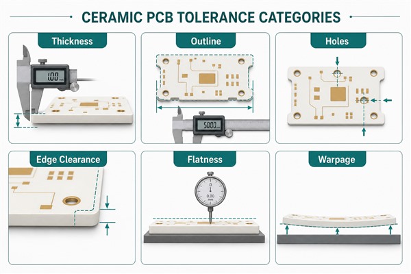
Ceramic PCB tolerance means the allowed variation between the design drawing and the finished ceramic circuit board. It covers ceramic substrate thickness, finished board outline, hole position, slot size, copper pattern registration, surface flatness, warpage and sometimes surface roughness. For a finished ceramic PCB, tolerance should be discussed as a complete manufacturing result, not only as a raw ceramic sheet value.
This is where many RFQs become unclear. A drawing may state a nominal board size and ceramic PCB thickness, but leave out whether the tolerance applies before or after metallization, whether copper thickness is included, which side is the reference surface, and which dimensions are critical to assembly. Those missing details force the supplier to quote conservatively or ask for clarification.
General ceramic PCB design rules are useful, but tolerance control deserves its own review. A layout can meet trace and spacing rules and still create problems if the outline is too tight for the housing, the hole-to-edge distance is weak, or the flatness requirement is not compatible with copper balance.
Quick Reference: Common Ceramic PCB Tolerance Areas
The first decision is to identify which dimensions actually affect the product. The table below separates common tolerance areas from the buyer decision behind them.
| Tolerance area | What it controls | Buyer note |
| Substrate thickness | Total ceramic body thickness, sometimes finished board thickness | Important for thermal interface, stack height and mechanical fit |
| Outline dimension | Length, width, round shape or custom profile | Tighter outline tolerance may require grinding or precision laser cutting |
| Hole and slot position | Mounting hole location, slot location and feature-to-feature distance | Critical for screws, alignment pins, connectors and housings |
| Copper registration | Copper pattern position relative to outline, holes and pads | Important for edge clearance, isolation and assembly alignment |
| Flatness and warpage | How far the finished board deviates from a flat reference plane | Critical for solder printing, die attach, baseplate contact and module assembly |
| Surface roughness | Texture of the ceramic or metallized surface | Relevant for thin film, bonding, sealing or high-precision mounting |
Ceramic PCB Thickness Tolerance
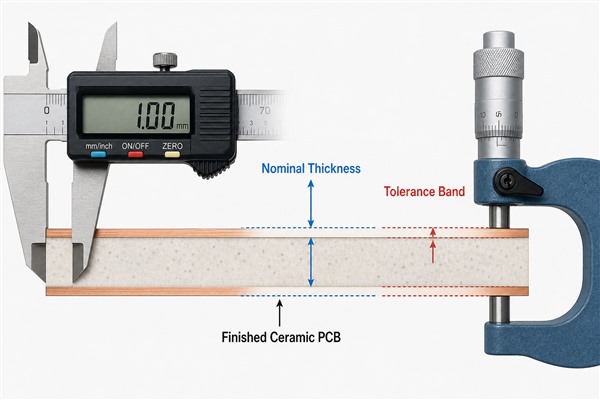
Ceramic PCB thickness tolerance should state whether the value refers to raw ceramic thickness, finished ceramic thickness, or total finished board thickness including copper and surface finish. This distinction matters because DPC, DBC, AMB, thick film and thin film processes add or bond different conductor structures onto the ceramic.
Common ceramic substrate thicknesses often include values such as 0.25 mm, 0.38 mm, 0.50 mm, 0.635 mm, 0.80 mm, 1.0 mm, 1.2 mm, 1.5 mm and 2.0 mm, but available ranges depend on material and process. Thin ceramic can help miniaturization and heat transfer, but it is easier to crack during handling. Thicker ceramic improves mechanical support and dielectric path, but may increase thermal resistance and processing cost.
For `tolerance pcb thickness`, `pcb tolerance thickness` and ceramic PCB thickness searches, the most useful answer is simple: do not copy a generic PCB tolerance standard blindly. For ceramic tolerance, define the function first. A power module substrate may need controlled thickness for thermal stack-up. A sensor carrier may need stable thickness for package height. A simple insulation plate may accept a wider tolerance if fit and thermal contact are not sensitive.
| Thickness requirement | When it matters | Practical specification advice |
| Standard substrate thickness | Most prototypes and cost-sensitive designs | Use a common available ceramic thickness unless assembly requires otherwise |
| Tight finished thickness | Thermal interface, stacked package, optical or mechanical height control | State measurement method and whether copper is included |
| Ground or polished thickness | Thin film, bonding, sealing or precision mounting | Expect higher cost and longer review because extra processing is needed |
| Loose thickness tolerance | Non-critical insulation or simple support parts | Use when mechanical fit and thermal path have enough margin |
Outline, Hole, Slot and Edge Tolerances
Outline tolerance controls whether the ceramic PCB fits the mechanical envelope. Hole and slot tolerance controls whether the board can be mounted without stress. Edge clearance protects copper features from chipping, isolation loss and mechanical damage during cutting or assembly.
For ceramic boards, sharp internal corners, very narrow bridges, holes close to the edge and long unsupported shapes should be reviewed early. Ceramic can be cut, lasered, punched or ground depending on material, thickness and volume, but each method has a different tolerance window and edge quality. A tolerance that is easy on a small rectangular alumina board may be difficult on a thin irregular AlN substrate.
Mounting holes deserve special attention. If screws, pins or clips apply force to the board, the drawing should define hole diameter, hole position, copper clearance around holes, minimum edge distance and whether metalized holes are required. For high-voltage ceramic PCB designs, copper-to-edge and copper-to-hole spacing should be checked together with creepage and clearance needs.
Flatness, Warpage and Assembly Risk
Flatness and warpage tolerance describe how much the finished ceramic PCB deviates from a reference plane. This is especially important for ceramic substrates used under power semiconductors, LEDs, laser diodes, sensors, RF modules and any assembly that requires uniform contact pressure.
Warpage can come from ceramic forming, sintering, grinding, asymmetric copper, thick copper, unbalanced patterns, brazing, reflow exposure or thermal cycling. Even if the raw ceramic is flat, the finished board can move after copper bonding or assembly heating. That is why flatness should be considered as a finished-board requirement, not only a raw-substrate property.
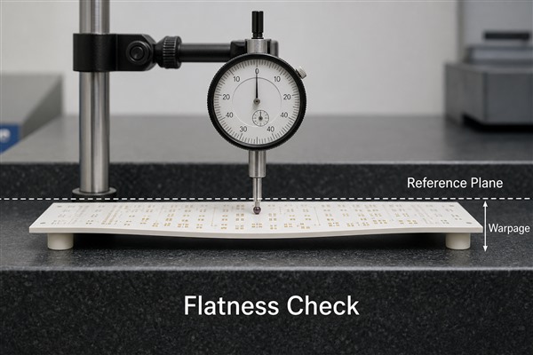
Flatness becomes a cost driver when the requirement is tighter than the process can naturally achieve. If the ceramic PCB is clamped to a heat sink with thermal grease, the flatness need may be different from a die-attach substrate that needs a very uniform bonding surface. The safest approach is to state the assembly method, contact area and acceptable gap rather than asking for an unrealistically tight number without context.
How Tolerances Change by Ceramic PCB Process
Ceramic PCB tolerance is process-dependent. DPC, DBC, AMB, thick film and thin film are not interchangeable manufacturing routes, so one tolerance table cannot cover every design. The process should be selected before the drawing tolerance is frozen.
| Process | Tolerance behavior | Best-fit tolerance focus |
| DPC ceramic PCB | Good for fine copper features and plated structures | Trace, spacing, via, pad and copper registration tolerance |
| DBC/DCB ceramic substrate | Thick bonded copper supports power paths but affects stress | Copper-to-edge distance, copper thickness, outline and warpage |
| AMB ceramic substrate | Often selected for power modules and stronger reliability needs | Copper symmetry, ceramic strength, flatness and thermal cycling tolerance |
| Thick film ceramic circuit | Printed conductor and fired paste behavior matters | Printed feature tolerance, resistor geometry and surface condition |
| Thin film ceramic substrate | Supports finer features but often needs smoother surfaces | Surface roughness, thickness, flatness and fine pattern alignment |
If copper thickness is part of the tolerance concern, review it together with the ceramic PCB copper thickness guide. Heavy copper can improve current capacity but can also make etching, spacing, warpage and stress control more difficult.
When Tight Tolerances Are Worth the Cost
Tight tolerance is worth the cost when it protects a real product function. Good examples include ceramic PCBs that must fit a machined housing, align with optical components, maintain die-attach flatness, control RF geometry, support high-voltage spacing, or keep stable contact with a heat sink or baseplate.
Tight tolerance is usually not worth the cost when the dimension does not affect assembly, performance or inspection. Over-specifying every dimension can increase grinding, inspection, sorting, yield loss and quotation time. It can also push the design toward a more expensive process when a standard tolerance would work.
| Situation | Use standard tolerance when... | Use tighter tolerance when... |
| Board outline | The board mounts with clearance in an open assembly | The ceramic fits into a tight pocket, slot or press-fit feature |
| Thickness | Stack height and heat path have design margin | Thermal interface, optical height or package height is sensitive |
| Hole position | Screws have clearance and do not force the ceramic | Alignment pins, connectors or clips define exact position |
| Flatness | The assembly uses compliant material and low contact pressure | Die attach, baseplate contact, solder printing or module sealing depends on it |
| Copper registration | Copper features are far from edge and mounting features | High voltage, edge plating, fine pads or mechanical alignment is critical |
What to Put on Your Ceramic PCB Drawing
A useful ceramic PCB drawing separates critical tolerances from reference dimensions. This helps the supplier protect the dimensions that matter while avoiding unnecessary inspection burden on dimensions that do not affect fit or function.
- Material and grade, such as alumina, AlN or Si3N4.
- Nominal ceramic thickness and whether thickness is raw ceramic or finished board.
- Finished copper thickness per side and surface finish.
- Critical outline dimensions with tolerances.
- Hole diameter, hole position and edge distance tolerance.
- Slot width, slot length, corner radius and minimum bridge width.
- Copper-to-edge, copper-to-hole and copper-to-slot clearance.
- Flatness or warpage requirement with measurement method if it is critical.
- Surface roughness requirement if bonding, sealing or thin film work depends on it.
- Inspection level, sample size or critical-to-quality dimensions.
For reliability-focused AMB or DBC projects, connect tolerance notes to use conditions. If the board will face thermal cycling, high-current switching or repeated power cycling, link the drawing requirements to the qualification plan. The article on thermal cycling fatigue analysis of AMB ceramic PCBs is a useful reference point for that discussion.
What to Send for a Tolerance Review and Quote
BSTCeramicPCB can review tolerance expectations more accurately when the RFQ package includes both drawing data and application context. Sending only a screenshot or a Gerber file without mechanical notes often leads to extra questions because the supplier cannot tell which tolerance is functional and which is only copied from a template.
- Gerber, ODB++ or CAD layout files.
- Mechanical drawing in PDF and editable format when available.
- Target ceramic material, ceramic PCB thickness and finished board thickness.
- Critical tolerances marked clearly on the drawing.
- Assembly method: soldering, die attach, wire bonding, screw mounting, clamping or heat sink contact.
- Operating temperature, voltage, current, thermal cycling or vibration requirements.
- Prototype quantity, expected production volume and inspection requirements.
A complete RFQ lets the supplier suggest practical alternatives. For example, a tolerance may be easier if the outline is adjusted, a slot radius is increased, a copper pattern is balanced, or the ceramic thickness moves to a standard available value. If you are preparing a custom ceramic PCB project, include these details before requesting final pricing.
FAQ
1. What is a ceramic PCB tolerance guide?
A ceramic PCB tolerance guide explains which dimensional, thickness, hole, copper and flatness tolerances should be controlled in a ceramic circuit board. It helps buyers specify realistic requirements before quotation.
2. Is ceramic PCB tolerance the same as FR4 PCB tolerance?
No. FR4 and ceramic PCBs use different materials and processes. Ceramic substrates are harder, more brittle and often processed by firing, grinding, laser cutting, metallization or copper bonding, so the tolerance review must be ceramic-specific.
3. What is the most important ceramic PCB thickness tolerance?
The most important thickness tolerance is the one that affects assembly or performance. For some boards, raw ceramic thickness is enough. For others, the finished thickness including copper and surface finish must be controlled.
4. What PCB tolerance standard should I use?
General PCB standards can help define documentation and inspection expectations, but they do not replace supplier-specific ceramic DFM review. Ceramic material, process route, copper structure and measurement method must be confirmed.
5. Why does ceramic PCB flatness matter?
Flatness affects solder paste printing, die attach, thermal interface contact, optical alignment and baseplate mounting. A board can meet outline tolerance but still create assembly problems if warpage is uncontrolled.
6. Can I request very tight ceramic tolerance?
Yes, but tight tolerance should be justified by function. It may require grinding, polishing, tighter inspection, lower yield or a different process, which can increase cost and lead time.
7. Which ceramic PCB tolerance affects cost most?
Cost often increases when outline, thickness, flatness, surface roughness or hole-position tolerances are tighter than standard process capability. Large panels, thin ceramic and heavy copper can also raise tolerance-control difficulty.
8. How should I specify hole tolerance on ceramic PCB?
Specify hole diameter, positional tolerance, plating or metallization requirement, copper clearance around the hole, and distance from the nearest board edge. Also state whether the hole is for mounting, alignment or electrical function.
9. Does copper thickness affect ceramic PCB tolerance?
Yes. Thick or asymmetric copper can affect etching allowance, copper registration, flatness and warpage. Copper thickness should be reviewed with ceramic thickness, board size and thermal cycling conditions.
10. What should I send to BSTCeramicPCB for tolerance review?
Send Gerber or CAD files, a mechanical drawing, ceramic material, ceramic PCB thickness, copper thickness, critical tolerances, assembly method, operating conditions, quantity and inspection requirements.
11. Can tolerance be relaxed after prototype testing?
Yes. If prototype results show that a dimension is not function-critical, it may be possible to relax that tolerance to reduce cost or lead time. The decision should be based on assembly and performance evidence.
12. How can I avoid over-specifying ceramic tolerance?
Mark only functional dimensions as critical, use standard available material thicknesses where possible, separate reference dimensions from controlled dimensions, and explain the assembly purpose behind each tight tolerance.
Conclusion
A practical ceramic PCB tolerance guide should help buyers decide which tolerances truly matter: thickness, outline, holes, slots, copper registration, flatness, warpage and surface condition. The right tolerance is not always the tightest one. It is the tolerance that protects assembly, thermal contact, electrical clearance and reliability with reasonable manufacturing cost.
If you are preparing a ceramic PCB, DPC, DBC or AMB substrate project, send your drawings, material target, ceramic PCB thickness, copper thickness, tolerance notes and operating conditions to BSTCeramicPCB for review. For quotation and engineering communication, contact sales@bstceramicpcb.com or use the contact BSTCeramicPCB page.
 Products
 About us
 Contact us



