






















































 HOME


-

Ceramic PCB for Humanoid Robot joint actuators
2026 04,07 -
LTCC PCB Surprises: What Most People Miss
2025 12,09 -
Step-by-Step Guide to DPC PCB Design for Sensor Systems
2025 12,03 -
Ceramic PCBs Essential Benefits and Applications
2025 12,01 -
How Al2O3 DPC Ceramic Substrate PCB Enhances Heat Dissipation in Modern Electronics?
2025 11,28 -
How to Choose Between Ceramic, FR4, and Metal Core PCBs
2025 11,27 -
DPC Ceramic PCB Materials: Surprising Science Inside
2025 11,26 -
Wire bondable 2-layer Alumina substrates PCB | Bstceramic PCB
2025 09,22 -
Silicon Nitride Substrate, Silicon Nitride Ceramic Substrate Formula
2025 05,08 -
What is thick film ceramic PCB?
2023 08,02
What Is Laser Trimming? Ceramic Resistor Cuts and Stability
Published:
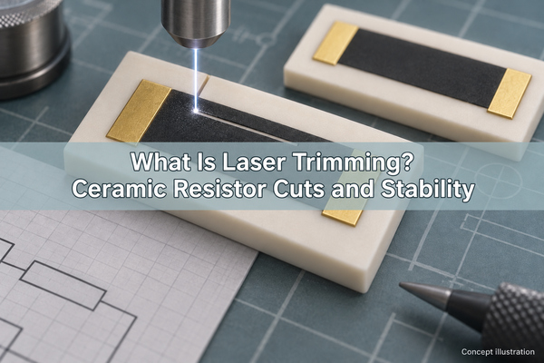
Laser trimming adjusts a ceramic resistor by removing a controlled amount of resistive film while its electrical value is monitored. The cut changes the current path, normally raising resistance toward a target. A successful trim must leave both the correct resistance and a sound remaining film: reaching the number on the meter does not prove that the resistor will remain stable after assembly, temperature exposure or operation.
What Is Laser Trimming on a Ceramic PCB?
On a ceramic circuit, laser trimming removes material from an integrated resistor, not from a separately soldered adjustment component. The narrow cleared track is called the kerf. The ceramic supports and insulates the circuit; it is not supposed to be cut through during resistor adjustment.
The laser trimming process corrects fabrication spread between resistor elements. It cannot repair a poorly bonded film or a cracked ceramic substrate.
In passive trimming, feedback comes from the measured resistance. In active or functional trimming, the circuit is powered and feedback comes from a parameter such as amplifier gain, bridge offset or frequency. A resistor that reaches its individual target may not produce the correct circuit output if other component tolerances matter. Conversely, a functionally adjusted circuit still needs acceptable resistor loading and electrical isolation.
Why Does Removing Resistor Material Increase Resistance?
Removing part of the conductive path restricts current flow. For an uncut rectangular film, the first estimate is R = Rs × L/W, where Rs is sheet resistance in ohms per square. A trim introduces a constriction or a longer path, so the simple rectangle calculation no longer describes the complete geometry.
Sheet resistance and bulk resistivity are not interchangeable. Sheet resistance already includes film thickness; for a uniform film, Rs = ρ/t. Firing or deposition variations, conductor overlap and contact regions also affect the fabricated value. The initial geometry therefore needs a practical upward adjustment range, not just a mathematically exact nominal value.
A simple planning example is a 900-ohm starting resistor intended for 1,000 ohms: the required increase is (1,000 - 900)/900 = 11.1%. This is an illustrative trim allowance, not a recommended universal starting percentage. If the same element already measures 1,020 ohms, ordinary film-removal trimming cannot bring it down to 1,000 ohms.
How Does Thick-Film Trimming Differ from Thin-Film Trimming?
The electrical objective is similar, but the material and process window are different. A thick film resistor is usually a fired resistive paste on ceramic; a thin film resistor is typically a deposited and patterned resistive layer. Neither technology can inherit the other's laser recipe solely because both use alumina.
| Process consideration | Thick film | Thin film |
|---|---|---|
| Before trimming | Paste selection, printed thickness and firing establish the starting distribution. | Deposited film, patterning and stabilization establish the starting distribution. |
| Material near the kerf | Local changes in the fired resistive network and glass-containing matrix can affect drift. | Alteration of the thin resistive layer, its interface or passivation can affect drift. |
| Geometry constraint | Keep enough remaining film for current and heat flow; account for print alignment. | Resolve the smaller film features without damaging neighboring conductors or underlying layers. |
| Process qualification | Evaluate the actual paste, firing profile, substrate and cut pattern together. | Evaluate the actual film system, protective layers and laser interaction together. |
Thick film resistor laser trimming is therefore part of the printed-resistor process, not a substitute for consistent printing and firing. For how the resistor is formed before adjustment, see our explanation of resistance printed on thick-film ceramic PCBs.
Laser trimming thin film resistor elements requires the same attention to the complete material stack. In our thin-film ceramic PCB fabrication, the circuit geometry and resistive-film requirements need to be specified together; a fine conductor line capability is not itself a permissible resistor kerf width.
Which Laser Trim Cut Should You Use?
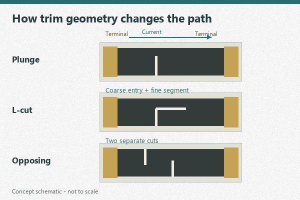
Choose the cut from the resistor's aspect ratio, required adjustment and allowable current concentration. A single plunge cut may be adequate for a small correction; an L-cut can separate a faster coarse adjustment from a less sensitive finishing segment. There is no cut shape that is best for every resistance, power or frequency.
| Cut pattern | Useful feature | Limitation to check |
|---|---|---|
| Plunge / straight cut | A simple cut enters from an edge, across part of the current path. | Resistance can become increasingly sensitive as the remaining neck narrows. |
| L-cut | An entering segment turns approximately along the original current direction for finer adjustment. | The turn, endpoint and remaining film must fit the actual resistor layout. |
| Two cuts / opposing cuts | Can provide additional adjustment or a coarse/fine strategy. | Spacing and cut lengths must not leave an excessively narrow or highly heated path. |
| Meander / serpentine trim | Creates a longer current route when a larger change is needed. | Local power density, noise and high-frequency behavior may change. |
Cut selection should also match circuit duty. A resistance that passes a DC check can still have unsuitable pulse loading or RF behavior after a large geometry change. For laser trimming resistors in a matched network, ratio tracking and thermal symmetry may matter more than making each nominal resistance independently exact.
What Makes a Good Resistor Trim Kerf?
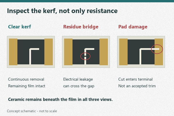
A useful kerf interrupts the unwanted electrical path cleanly without damaging the termination, neighboring circuit or ceramic support. Appearance alone is insufficient: residue or redeposited material can leave leakage across a gap that looks open under low magnification.
- Continuous clearance: avoid islands or bridges of resistive material across the intended cut.
- Controlled endpoint: retain a sound current-carrying path rather than extending the cut until the resistor is nearly severed.
- Termination clearance: keep the trim away from conductor overlaps unless the approved design explicitly provides a trim region there.
- Limited local damage: inspect for chipping, cracking, lifting or an excessive heat-affected region.
- Electrical isolation: verify the kerf and adjacent nodes at conditions appropriate to the circuit voltage and resistance range.
Focus, pulse energy, repetition rate, scanning speed and pulse overlap interact. Too little removal can leave conducting residue; excessive energy can damage material beneath or beside the kerf. A numerical laser setting without the film system, optics and process conditions is not a transferable manufacturing specification.
How Is Resistance Measured During Trimming?
The laser resistor trimming system measures an accessible electrical path and uses that feedback to stop material removal. Test pads and circuit isolation must be designed before fabrication; probing an arbitrary pair of pads may measure parallel resistors or semiconductor paths instead of the intended element.
For low resistance or tight tolerances, four-wire Kelvin measurement separates the current leads from the voltage-sense leads and reduces lead/contact resistance error. High-value elements instead demand particular attention to leakage, contamination and fixture insulation. Test current must be low enough to avoid a self-heating error, while still giving the instrument a usable signal.
A laser trimming machine's measurement resolution is not the complete uncertainty. Probe repeatability, instrument calibration, substrate temperature, settling time and final verification conditions all contribute. In our thick-film ceramic circuits with integrated resistors, resistor identifiers and accessible test nodes need to agree with the circuit drawing so measured values can be assigned to the correct elements.
How Can You Avoid Overshooting the Target Resistance?
Allow trim headroom in the fabricated resistor and reduce the electrical change per step near the target. A late stop cannot restore film that has already been removed.
- Measure the starting value and reject elements already above the permitted trim window.
- Use a qualified coarse cut to approach the target without consuming the entire adjustment region.
- Change to a less sensitive finishing path or smaller adjustment increments.
- Allow for measurement latency and the resistance change associated with the final laser pulses.
- Verify the cooled or settled value under the specified final-test conditions.
The stop threshold may differ from the final acceptance target if the process has a repeatable short-term shift. That offset must come from measured process characterization, not an assumed percentage. If starting values require unusually deep cuts, correct the resistor geometry, paste/deposition process or trim allowance instead of relying on aggressive trimming to recover every part.
Does a Tight Trim Tolerance Guarantee Long-Term Stability?
No. Initial tolerance describes the resistance error at a defined measurement condition. Long-term stability describes the change after time or stress; temperature coefficient of resistance, or TCR, describes a different relationship with temperature. These requirements need separate limits.
| Requirement | What to state | What it does not prove |
|---|---|---|
| Initial resistance tolerance | Target, permitted error, temperature and test current | Life-test drift or humidity resistance |
| TCR | Temperature interval, method and ppm/K limit | Permanent change after a heat cycle |
| Load-life stability | Applied load, ambient, duration and allowable change | Performance at a different load or temperature |
| Ratio stability | Which resistors form the ratio and allowable tracking error | Absolute accuracy of each element |
For a 10,000-ohm element, a 0.1% initial tolerance corresponds to +/-10 ohms at the stated reference condition. A separate 0.2% drift allowance corresponds to a further 20-ohm change relative to the specified drift baseline. These illustrative limits cannot be treated as one interchangeable accuracy claim.
Why Can Resistance Drift After Laser Trimming?
Post-trim drift can come from the altered film beside the kerf, residual stress, contamination, protective-layer changes or later thermal processing. Narrow remaining paths can also concentrate current and heat during service. The target resistance can be correct even when the geometry leaves too little reliability margin.
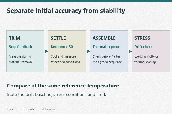
Short-term thermal settling is not the same as permanent aging. First compare measurements at the same reference temperature and after the same settling period. Then evaluate the change after assembly exposure, thermal cycling, humidity or load life. Measuring one part hot and the other cold confounds TCR with irreversible drift.
Thin film adhesion and ceramic surface roughness also belong in the material-system assessment when film integrity is in question. A nominally narrow kerf cannot compensate for a poorly bonded film. Passivation and any post-trim stabilization treatment must be qualified for the chosen resistor system; adding a coating or repeating a high-temperature firing step is not an automatic cure.
How Do You Validate a Trimmed Ceramic Resistor?
Validate the finished resistor in the condition that will actually be delivered and used. Begin with baseline electrical and visual checks, then apply the stresses justified by the application. Qualification samples should include the largest intended trim corrections, not only lightly trimmed elements.
- Baseline: resistor ID, starting value, settled post-trim value, temperature, measurement current and instrument setup.
- Kerf inspection: cut location, bridges, film damage and clearance to terminations.
- Assembly exposure: resistance before and after the agreed soldering, bonding or curing sequence.
- Operating stress: power, pulse load, temperature and humidity where relevant, with explicit duration and acceptance limits.
- Network behavior: ratio, offset or gain where circuit function, rather than a single resistance, is the acceptance criterion.
Use a defined drift calculation, such as ΔR/R0 = (Rafter - R0)/R0, and identify R0. It might be the settled post-trim value or the post-assembly value, depending on the agreed test. Mixing those baselines makes otherwise valid results impossible to compare.
What Should a Laser-Trimmable Resistor Drawing Specify?
Specify the element, its adjustment region and its acceptance conditions together. A note saying only "trim to 0.1%" leaves uncertainty about temperature, power, network connections and the state of the circuit at final test.
- Resistor map with nominal values, tolerances and any matched ratios.
- Substrate and resistive-film system, conductor overlaps and permitted trim area.
- Probe pads, isolation requirements and passive or functional adjustment method.
- Reference temperature, measurement current, settling time and final-test stage.
- Operating voltage/power, pulse conditions, TCR and allowable post-stress drift.
- Protective coating, assembly heat exposure and inspection/test records required.
At BSTCeramicPCB, we manufacture thick-film and thin-film ceramic circuits. Our thin-film process supports laser-trimmable resistance accuracy of +/-0.1%, with +/-0.05% requirements subject to special project review. Those figures describe resistance accuracy, not a blanket TCR or lifetime-drift guarantee. We need the film, layout and test conditions before confirming an applicable target.
For custom thick-film ceramic circuits for communication electronics, provide the resistor and conductor layers together rather than treating the cut as an isolated finishing detail. Send the drawing, resistor list, quantity and operating conditions to sales@bstceramicpcb.com so we can review a suitable ceramic-circuit manufacturing route and quotation.
Laser Trimming FAQs
Can any finished ceramic resistor be laser trimmed?
No. Laser-trimmable resistors need accessible film, compatible materials, an adequate adjustment region and a usable measurement path. Trimming through an unsuitable coating or modifying a standard component without qualification can damage protection or change its ratings.
Is resistor trimming the same as ceramic laser scribing?
No. Resistor trimming changes the electrical film geometry. Ceramic scribing prepares the substrate for separation or outlines; it has a different depth, purpose and acceptance criterion.
Can an extra trim repair resistance that has drifted?
Only if the required correction is upward and the design still has a qualified trim allowance. A second cut does not remove the cause of an unstable film. Rework requires another electrical and reliability assessment, not just another nominal-value check.
Controlled laser trimming combines a suitable starting resistor, a clean cut and repeatable measurement. The accepted result is a resistor that meets both its initial electrical target and the separately defined stability requirements.
 Products
 About us
 Contact us



