




















































 HOME


-

4-Layer Alumina PCB: Stackup, Design Rules & Manufacturing Guide
2026 10,29 -
Aluminum Nitride Thermal Conductivity vs Temperature
2026 10,21 -
Wire Bonding EPIG Thickness: Selecting Pd/Au for Ceramic Bond Pads
2026 10,19 -
When Does a Thin-Film Circuit Need a Polished Alumina Substrate?
2026 10,18 -
Ceramic PCB for Humanoid Robot joint actuators
2026 04,07 -
LTCC PCB Surprises: What Most People Miss
2025 12,09 -
Step-by-Step Guide to DPC PCB Design for Sensor Systems
2025 12,03 -
Ceramic PCBs Essential Benefits and Applications
2025 12,01 -
How Al2O3 DPC Ceramic Substrate PCB Enhances Heat Dissipation in Modern Electronics?
2025 11,28 -
How to Choose Between Ceramic, FR4, and Metal Core PCBs
2025 11,27 -
DPC Ceramic PCB Materials: Surprising Science Inside
2025 11,26 -
Wire bondable 2-layer Alumina substrates PCB | Bstceramic PCB
2025 09,22 -
Silicon Nitride Substrate, Silicon Nitride Ceramic Substrate Formula
2025 05,08 -
What is thick film ceramic PCB?
2023 08,02
4-Layer Alumina PCB: Stackup, Design Rules & Manufacturing Guide
Published:
A 4-layer alumina PCB offers more routing space and electrical isolation than a conventional single-layer ceramic circuit. But can your four-layer design actually be manufactured? Incorrect dielectric spacing, interlayer connections, or metallization can cause problems that are difficult to correct once production begins.
The right stackup and design rules can prevent those problems before fabrication. BSTCeramicPCB provides custom 4-layer alumina PCB manufacturing, free DFM review, and assembly services to help customers verify their designs, reduce prototype revisions, and move into production with fewer delays.
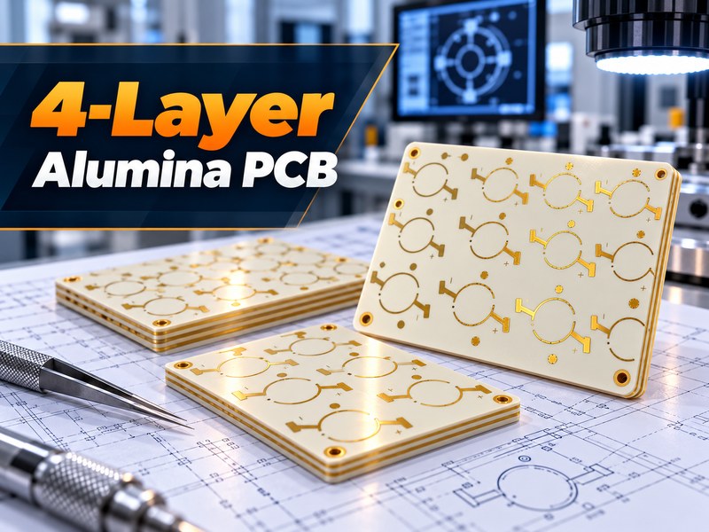
What Are the Common Stackup Configurations for a 4-Layer Alumina PCB?
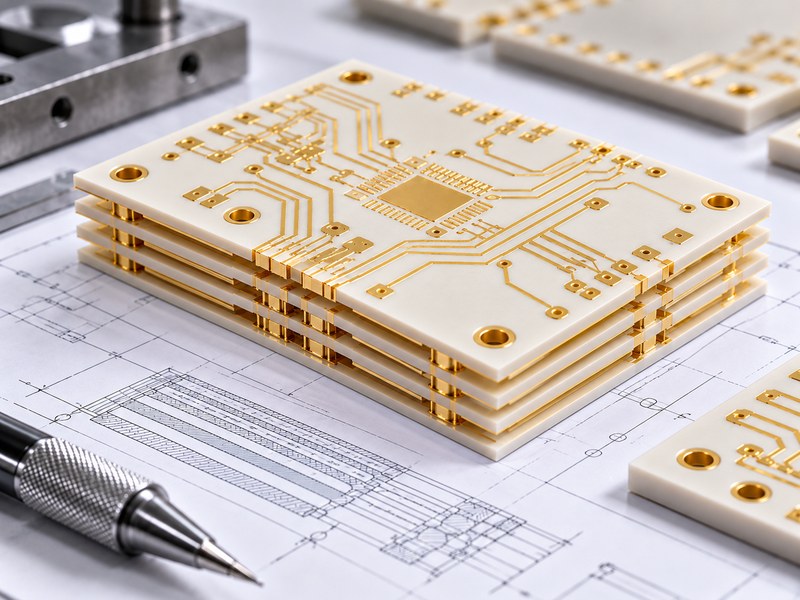
A 4-layer alumina PCB stackup uses four patterned conductor levels separated by insulating dielectric material. In multilayer thick-film construction, these levels are printed and fired sequentially on a single alumina substrate.
A typical single-sided four-layer arrangement is shown below.
| Layer | Circuit Function | Design Considerations |
|---|---|---|
| L4 – Top conductor | Component pads, external connections, and surface signal routing | Pad finish, solderability, component clearance |
| L3 – Upper internal conductor | Additional signal routing or ground connections | Dielectric separation, conductor alignment |
| L2 – Lower internal conductor | Power distribution, reference patterns, or signal routing | Conductor resistance, insulation, registration |
| L1 – Base conductor | Buried routing and interlayer connections | Conductor adhesion, connection continuity |
| Alumina substrate | Mechanical support and electrical insulation | Purity, thickness, flatness, and dimensions |
Printed dielectric separates the adjacent conductor levels. Electrical connections pass through designated openings in the dielectric, allowing selected circuits to connect between layers.
For example, when component pads occupy most of the top surface, additional signals can be routed through the internal conductor levels. Ground connections may also be distributed between layers, provided the dielectric thickness and conductor geometry satisfy the electrical requirements.
Two construction details are especially important:
- Single-sided multilayer thick film: All four conductor levels are built on one face of a fired alumina substrate. This is the relevant four-layer thick-film construction offered by BSTCeramicPCB.
- Multilayer HTCC: Conductors are embedded between ceramic layers and co-fired into a monolithic body. This requires a different material system, metallization process, and design review.
A 4-layer alumina PCB is therefore not simply an FR4 stackup made from ceramic. The conductor arrangement, insulation system, and interlayer connections must match the chosen manufacturing process.
How Do Alumina Purity and Substrate Thickness Affect 4-Layer PCB Performance?
96% alumina is a common material for multilayer thick-film circuits, offering electrical insulation, thermal stability, and compatibility with established conductor and dielectric systems.
Higher-purity grades, such as 99.6% Al₂O₃, may be appropriate for certain electronic packaging applications, but they are not automatically necessary for a four-layer circuit. Material selection should account for surface properties, thermal requirements, and metallization compatibility.
Substrate thickness also affects the finished product:
- 0.25–0.38 mm: Suitable for compact, low-profile circuits where substrate handling and mechanical support can be controlled.
- 0.50–0.635 mm: Common choices for thick-film ceramic circuits that require a balance of rigidity and compact dimensions.
- 0.80–1.00 mm: Useful where additional mechanical support is needed, although a thicker substrate increases the distance heat must travel through the ceramic.
These are substrate thickness options, not guaranteed finished dimensions for every four-layer construction. Printed conductors, dielectric layers, and protective coatings can add to the final thickness.
For heat-generating components, substrate thickness, conductor layout, component attachment, and heat-sink contact all affect thermal performance. Material purity alone cannot determine the operating temperature.
What Are the Key Design Rules for a 4-Layer Alumina PCB?
Conductor spacing, dielectric insulation, interlayer connection geometry, and layer registration are the most important design rules for a 4-layer alumina PCB.
Unlike FR4 manufacturing, thick-film fabrication involves screen printing and repeated firing. Conductor dimensions and dielectric coverage must therefore account for printing accuracy and alignment between successive layers.
BSTCeramicPCB publishes the following general thick-film references. The complete four-layer construction still requires project-specific approval.
| Design Parameter | Reference or Requirement | What to Verify Before Manufacturing |
|---|---|---|
| Prototype line width / spacing | 0.20 / 0.20 mm published thick-film reference | Whether the geometry is achievable on the required conductor levels |
| Production line width / spacing | ≥0.25 / 0.25 mm published thick-film reference | Suitability for the complete four-layer construction |
| Alumina substrate thickness | 0.635 mm common reference | Finished thickness, flatness, and handling requirements |
| Interlayer via dimensions | Process-dependent | Connection opening, conductor overlap, and registration allowance |
| Dielectric thickness | Material- and application-dependent | Working voltage, insulation resistance, and dielectric coverage |
| Conductor-to-edge clearance | Determined by the cutting method and board geometry | Risk of damaged traces, edge cracking, and exposed conductors |
| Metallization | Compatible thick-film metal paste | Electrical resistance, solderability, bonding, and firing compatibility |
The published line widths are general thick-film references, not guaranteed minimum dimensions for every four-layer alumina PCB.
Several design issues require particular attention.
Step 1: Interlayer via alignment
An interlayer connection must overlap the conductor patterns above and below the dielectric opening. If the opening is too small or the pads do not allow sufficient registration tolerance, the resulting connection may be incomplete.
Where several levels require connection, the placement of successive via openings should also be reviewed. Directly stacked connections should not be assumed feasible without process approval.
Step 2: Dielectric insulation between conductors
Each conductor crossover requires sufficient dielectric coverage to prevent unwanted electrical contact. Inadequate coverage, printing defects, or dielectric pinholes can cause shorts or insulation failure.
For circuits operating at elevated voltage, specify the working voltage, required insulation resistance, and applicable withstand-voltage test. These conditions determine the appropriate insulation design.
Step 3: Conductor resistance and current capacity
Thick-film conductors are generally much thinner than heavy-copper PCB conductors. A narrow trace carrying substantial current can generate excessive heat or voltage drop.
Conductor width, material, fired thickness, and routing length should be considered together. A design requiring large current-carrying conductors may be better suited to another ceramic metallization process.
Step 4: Metallization and component attachment
Pad materials must match the intended assembly method. SMT soldering, gold wire bonding, and exposed contact pads can require different conductor finishes.
BSTCeramicPCB's thick-film guidance also identifies specific material limitations for interlayer connections. Designs combining gold-based conductors with silver-based via materials require separate compatibility review.
Step 5: Mechanical and thermal clearances
Ceramic substrates resist bending and are vulnerable to cracking under concentrated mechanical loads. Avoid placing critical conductors close to mounting points, cutting edges, or regions exposed to assembly stress.
Thermal expansion differences between alumina, metallic conductors, solder joints, and attached components should also be considered in high-temperature applications.
How Are 4-Layer Alumina Ceramic PCBs Manufactured?
4-layer alumina ceramic PCBs are commonly manufactured using sequential thick-film printing and firing, with each conductor and dielectric level formed in a controlled order.
The main manufacturing steps are:
-
Substrate preparation: Select the required alumina grade and thickness. Inspect the ceramic for flatness, dimensional accuracy, contamination, and visible defects.
-
First conductor printing: Screen-print the initial conductor pattern using a compatible metal paste. Dry and fire the printed layer to form the conductive circuit.
-
Dielectric formation: Print insulating dielectric over the required regions, leaving openings for electrical connections. Process the dielectric according to the selected material system.
-
Interlayer connection and conductor printing: Form conductive connections through the dielectric openings and print the next circuit pattern. Alignment must be maintained between the conductor and dielectric layers.
-
Four-layer buildup: Repeat the conductor and dielectric operations until all four conductive levels are complete. Each firing stage must remain compatible with the previously formed layers.
-
Finishing and inspection: Complete external pads, protective layers, and substrate profiling. Inspect critical dimensions and perform the specified electrical tests.
Not every four-layer ceramic circuit uses this process.
For HTCC multilayer alumina PCBs, conductor patterns are formed on unfired ceramic tapes. The tapes are aligned, laminated, and co-fired, creating buried interconnections within the ceramic body. Refractory-metal conductors, typically tungsten or molybdenum, are commonly used.
HTCC has different shrinkage, via, and conductor requirements. A design intended for thick-film alumina cannot be transferred directly to HTCC without adapting the stackup and manufacturing files.
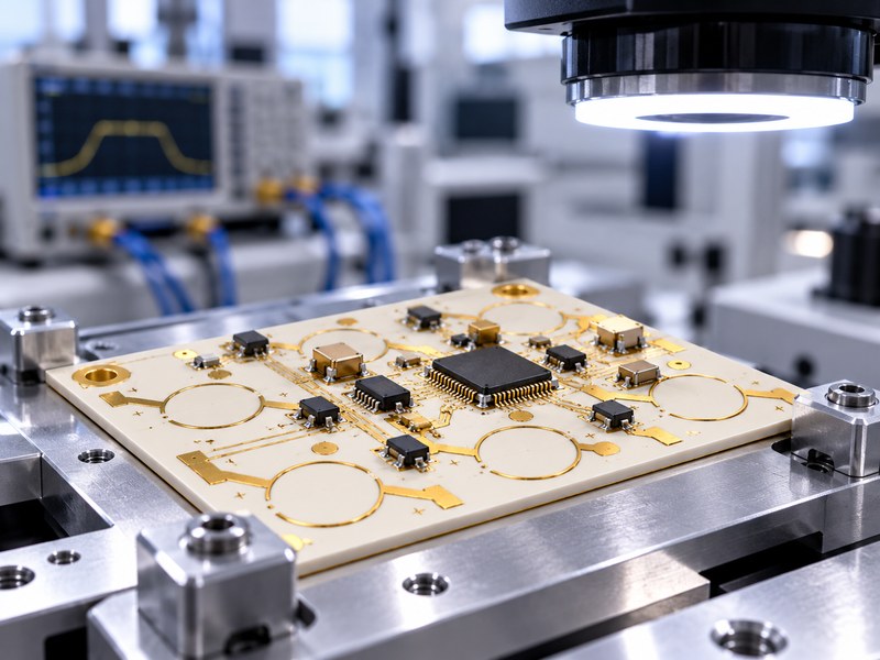
What Are the Main Applications of 4-Layer Alumina PCBs?
4-layer alumina PCBs are most useful when additional conductor levels solve routing, isolation, or packaging constraints that cannot be addressed efficiently with a simpler ceramic circuit.
Typical applications include:
- RF and communication modules: Four conductor levels can accommodate signal routing, reference connections, and bias networks in compact modules. Controlled-impedance designs require careful evaluation of dielectric properties and conductor geometry.
- Industrial sensor electronics: Multilayer routing helps accommodate sensor connections, signal-conditioning circuits, and electrical isolation within limited space, particularly in equipment operating at elevated temperatures.
- Medical diagnostic equipment: Alumina multilayer circuits can support compact electronic assemblies where stable insulation, controlled assembly conditions, and dimensional accuracy are required.
- Aerospace and high-temperature electronics: Ceramic multilayer circuits can serve electronic packages exposed to demanding operating environments, provided the finished assembly meets the relevant qualification requirements.
A four-layer construction is not always necessary. If the circuit fits within one or two conductor levels without compromising electrical performance, a simpler alumina substrate may be sufficient.
Likewise, applications requiring thick copper conductors and substantial current capacity may benefit more from DBC or AMB ceramic PCB technology than conventional multilayer thick film.
How Is the Quality and Reliability of a 4-Layer Alumina PCB Verified?
A 4-layer alumina PCB requires electrical and structural verification because internal connections cannot be fully inspected after fabrication.
The inspection plan should address conductor defects, insulation failures, substrate damage, and the integrity of interlayer connections.
Key checks include:
- Dimensional inspection: Verify finished dimensions, substrate thickness, conductor features, and critical hole locations against the approved drawings.
- Electrical continuity testing: Detect open conductors and incomplete interlayer connections.
- Insulation resistance testing: Confirm electrical isolation between independent circuits under the specified test conditions.
- Metallization inspection: Check exposed pads, conductor patterns, surface defects, and applicable adhesion requirements.
- Cross-section examination: Assess selected qualification samples for interlayer connection quality, conductor overlap, and dielectric coverage where needed.
- Thermal reliability testing: Evaluate the substrate and metallization under project-specific thermal cycling or exposure requirements.
Electrical testing should use agreed acceptance limits rather than generic pass/fail criteria. The required insulation voltage, resistance limits, and test coverage depend on the circuit and its operating environment.
If the ceramic PCB is supplied as an assembled board, first-article inspection, solder joint assessment, and functional testing can be added according to the assembly specification.
What Is the Typical Lead Time for a 4-Layer Alumina PCB?
BSTCeramicPCB lists a normal lead time of approximately 3–4 weeks for 4-layer thick-film ceramic PCB prototypes, with expedited options available for suitable orders after feasibility and scheduling confirmation.
The actual delivery schedule depends on several requirements:
- Material availability: Nonstandard alumina grades or substrate thicknesses may need additional preparation.
- Circuit complexity: Fine conductors, multiple dielectric operations, and demanding interlayer alignment can increase processing time.
- Special metallization: Wire-bondable finishes or other attachment requirements may involve additional production steps.
- Qualification testing: Thermal cycling, cross-section evaluation, or other project-specific tests can extend the approval schedule.
Providing complete manufacturing files and confirming the stackup before production helps avoid engineering changes that could affect the delivery date.
Why Choose BSTCeramicPCB for Custom 4-Layer Alumina PCB Manufacturing?
BSTCeramicPCB helps customers turn manufacturable ceramic circuit designs into finished boards and assemblies, with engineering support before fabrication and testing options matched to the project.
For your 4-layer alumina PCB project, you can benefit from:
- Identify design problems before production: Our free DFM review examines conductor spacing, layer alignment, dielectric openings, metallization, and substrate requirements. You can address potential manufacturing problems before committing to prototype fabrication.
- Get a manufacturing solution that fits your design: We assess whether your circuit can use our four-layer thick-film process and identify limitations that may require changes to the stackup or conductor arrangement.
- Source bare boards and assembly from one supplier: We provide ceramic PCB fabrication, component sourcing, SMT assembly, first-article inspection, and functional testing for compatible projects. This helps avoid mismatches between the ceramic pad finish and the intended component attachment process.
- Reduce unnecessary prototype revisions: Reviewing the material, circuit geometry, and assembly requirements together helps identify incompatible specifications before manufacturing. You receive engineering feedback on the changes needed to make the design practical.
- Plan your project around a defined lead time: Our published four-layer thick-film prototype lead time is approximately 3–4 weeks, with expedited options subject to project requirements. We confirm the manufacturing schedule after reviewing your files.
- Request inspection and quality documentation: Electrical testing, dimensional inspection, and other agreed verification methods can be included according to your application requirements. Relevant quality certification information can also be provided for review.
Whether you need bare 4-layer alumina boards or assembled ceramic circuits, BSTCeramicPCB can review your manufacturing files and provide a project-specific fabrication solution.
FAQs About 4-Layer Alumina PCBs
Q1. Can an Existing 4-Layer FR4 PCB Design Be Converted to Alumina?
A1. Yes, but it normally requires changes to the stackup and layout. Alumina has different dielectric properties, conductor materials, interlayer connections, and mechanical constraints from FR4.
Q2. Can SMT and Gold Wire Bonding Be Used on the Same Alumina PCB?
A2. Yes, if the metallization and pad finishes are compatible with both attachment methods. Separate pad specifications may be necessary for soldering and wire bonding.
Q3. How Can Ceramic PCB Cracking Be Prevented During Assembly?
A3. Use suitable fixtures, avoid concentrated clamping loads, and control thermal stress during assembly. Mounting geometry and expansion differences between ceramic and attached components also need attention.
Q4. Can 4-Layer Alumina PCBs Be Manufactured in Arrays?
A4. Array fabrication may be possible depending on substrate dimensions, thickness, and the separation method. Ceramic panelization must account for cracking and edge damage during singulation.
Q5. Are Lead-Free Soldering Processes Compatible with Alumina Ceramic PCBs?
A5. Yes, when the metallization, solder alloy, and reflow profile are compatible. The solder joints and pad adhesion must withstand the required thermal exposure.
Q6. Can Components Be Reworked on an Alumina Ceramic PCB?
A6. Some components can be replaced using controlled rework methods. Excessive local heating, mechanical force, or repeated thermal cycling may damage the ceramic or conductor pads.
How Can You Request a Custom 4-Layer Alumina PCB Quote?
BSTCeramicPCB provides custom 4-layer alumina PCB fabrication, prototyping, and assembly services for industrial, RF, electronic packaging, and high-reliability applications.
For a manufacturing review and quotation, please send:
- Gerber files and stackup: Four conductor layers, dielectric arrangement, and interlayer connections.
- Material specifications: Alumina grade, substrate thickness, finished dimensions, and tolerances.
- Circuit requirements: Conductor geometry, metallization, insulation requirements, and surface finish.
- Order details: Quantity, required delivery date, and delivery location.
- Assembly information: BOM, component placement data, and testing requirements, if applicable.
Email sales@bstceramicpcb.com to request a free DFM review and quotation. Our team can help you confirm manufacturing feasibility and obtain custom 4-layer alumina PCB boards that match your project requirements.
 Products
 About us
 Contact us