






















































 HOME
HOME

-

Ceramic PCB for Humanoid Robot joint actuators
2026 04,07 -
LTCC PCB Surprises: What Most People Miss
2025 12,09 -
Step-by-Step Guide to DPC PCB Design for Sensor Systems
2025 12,03 -
Ceramic PCBs Essential Benefits and Applications
2025 12,01 -
How Al2O3 DPC Ceramic Substrate PCB Enhances Heat Dissipation in Modern Electronics?
2025 11,28 -
How to Choose Between Ceramic, FR4, and Metal Core PCBs
2025 11,27 -
DPC Ceramic PCB Materials: Surprising Science Inside
2025 11,26 -
Wire bondable 2-layer Alumina substrates PCB | Bstceramic PCB
2025 09,22 -
Silicon Nitride Substrate, Silicon Nitride Ceramic Substrate Formula
2025 05,08 -
What is thick film ceramic PCB?
2023 08,02
Ceramic Hardness: Tests, Values and PCB Design Effects
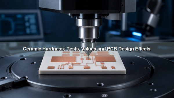
Ceramic hardness is a material's resistance to localized indentation, scratching, and wear. Advanced ceramic PCB substrates are much harder than most polymers and often harder than steels by indentation, but hardness does not measure resistance to cracking. Material chemistry, purity, pores, grain boundaries, surface preparation, indenter geometry, and test load all affect the reported value.
What Is Ceramic Hardness?
Ceramic hardness measures how strongly a surface resists permanent local deformation when a harder indenter presses into it. The result is calculated from the applied load and the size or depth of the residual indentation, depending on the test method.
For ceramic PCB work, hardness influences wear resistance, grinding, lapping, laser interaction, scribing, drilling, surface preparation, and edge finishing. It does not by itself predict whether a substrate will survive bending, impact, thermal shock, or a concentrated mounting load.
Why Do Ceramics Have High Hardness?
Ceramics are hard because their atoms are joined by strong ionic and covalent bonds in rigid crystal structures. Moving a dislocation or permanently rearranging the lattice requires substantial energy, so the surface resists plastic indentation.
This same limited plasticity explains why a hard ceramic can also be brittle. Metals can yield and redistribute a local stress; a ceramic has less ability to deform plastically, so a flaw may concentrate tensile stress and start a crack.
Which Hardness Tests Are Used for Advanced Ceramics?
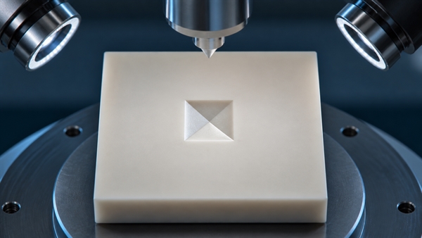
Vickers and Knoop indentation tests are commonly used for advanced ceramics. A diamond indenter is pressed into a polished surface under a specified force, and the indentation geometry is measured. ASTM C1327 covers Vickers indentation hardness for advanced ceramics.
| Method | Typical use | Important limitation |
|---|---|---|
| Vickers | General advanced-ceramic comparison | Value depends on load, surface preparation and crack-free measurement |
| Knoop | Thin sections, coatings or anisotropic materials | Direction and surface finish can affect the long indentation |
| Mohs | Relative scratch ranking | Too coarse for precise PCB-grade comparison |
| Rockwell | Common for metals and some ceramics | HRC values should not be directly converted to Vickers for all ceramics |
A hardness number is meaningful only when the method, load, specimen preparation, temperature, and material grade are stated.
What Is the Hardness of Ceramic Materials?
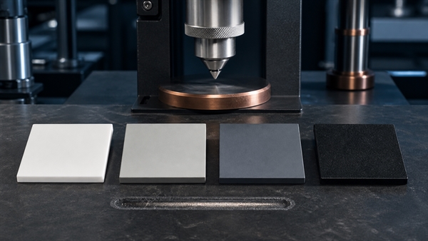
Hardness varies widely across ceramic families and commercial grades. The following Vickers examples are typical values published for specific Kyocera materials at the stated HV9.807N condition; they are reference points, not universal specifications.
| Material family | Example Vickers hardness | Practical interpretation |
|---|---|---|
| Alumina grades | about 12.0–17.5 GPa | High wear resistance; grade and purity matter |
| Aluminum nitride | about 10.4–11.2 GPa | Electrically insulating with high thermal conductivity |
| Silicon nitride | about 13.8–14.0 GPa | Combines hardness with comparatively high fracture toughness |
| Silicon carbide | about 22–23 GPa | Extremely hard, with difficult machining |
| Zirconia grades | about 10.7–12.7 GPa | Lower hardness than SiC but relatively high toughness |
Use the exact supplier datasheet and test method for design. A broad phrase such as “the hardness of ceramic materials” cannot be reduced to one number.
Is Ceramic Harder Than Steel?
Many advanced ceramics are harder than common steels in indentation and wear tests, but steel is usually much tougher and more tolerant of impact or edge loading. Hardness comparisons therefore answer only one part of the mechanical design question.
A steel mounting plate may scratch before an alumina substrate does, yet the steel can bend without breaking while the ceramic may crack from a small edge chip or an uneven clamp. Ceramic PCB fixtures should spread load and protect edges instead of relying on hardness as proof of damage tolerance.
Hardness, Strength, Toughness and Stiffness Are Different
These mechanical properties describe separate failure modes.
| Property | What it measures | PCB implication |
|---|---|---|
| Hardness | Resistance to local indentation and wear | Machining, scratching and surface durability |
| Flexural strength | Stress at fracture in bending under a stated test | Board bending and handling limits |
| Fracture toughness | Resistance to crack growth | Sensitivity to flaws, chips and thermal shock |
| Elastic modulus | Resistance to elastic deformation | Deflection and stress transfer to components |
High hardness does not compensate for a low fracture-toughness margin. A robust design reviews all four properties together with substrate thickness, geometry, defects, temperature, and assembly constraints.
How Do Purity, Grain Size and Porosity Change Hardness?
Purity, secondary phases, grain size, and porosity change the area that actually carries the indenter load. Pores reduce load-bearing material and can distort an indentation. Glassy grain-boundary phases may be softer than alumina grains, while abnormal grain growth can produce nonuniform local behavior.
Higher-purity alumina grades often show higher hardness, but the trend is not guaranteed across every manufacturing route. A double-sided Al2O3 DPC ceramic circuit board for laser equipment should be evaluated with its actual grade, density, surface finish, and edge process rather than a generic alumina value.
The BSTCeramicPCB guides to different grades of alumina and alumina density explain why purity percentage alone is not a complete specification.
How Does Ceramic Hardness Affect Laser Cutting and Drilling?
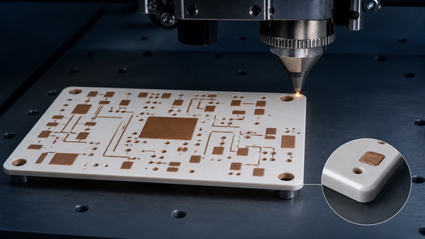
High hardness makes conventional cutting-tool wear severe, so ceramic substrates are commonly shaped by laser processing, grinding, dicing, ultrasonic machining, or diamond tooling. Each process can introduce a different combination of taper, roughness, microcracks, recast material, heat-affected zones, and edge chips.
Hole diameter, substrate thickness, pitch, hole-to-edge distance, corner radius, and acceptable chipping must be reviewed together. For a fine-feature alumina DPC ceramic substrate PCB for LED applications, small circuit geometry does not remove the need for realistic ceramic machining tolerances. See how to cut alumina ceramic substrates for process considerations.
How Does Hardness Affect Metallization and Surface Finish?
Hardness affects how a ceramic surface is lapped, polished, roughened, cleaned, and activated before metallization. A very smooth surface can support fine features, but adhesion depends on the complete interface process rather than roughness alone. Excessive mechanical preparation can introduce subsurface damage.
Thick film, DPC, thin film, DBC, and AMB use different adhesion mechanisms and conductor thicknesses. Surface finish must therefore be specified for the selected metallization route and verified after cleaning, firing, plating, bonding, or brazing.
How Can Edge Chipping and Assembly Cracks Be Reduced?
Edge damage is reduced by avoiding sharp internal corners, providing adequate hole-to-edge distance, controlling laser and dicing parameters, and supporting the panel during handling. Inspection should focus on critical holes, notches, corners, and metallized edges where tensile stress concentrates.
During assembly, use flat support, controlled clamp force, suitable fastener isolation, and an interface that accommodates coefficient-of-thermal-expansion mismatch. Heavy components or busbars should not transfer a point load into an unsupported ceramic edge.
Which Ceramic Substrate Fits Mechanical and Wear Loads?
The hardest ceramic is not automatically the best PCB substrate. Alumina offers a mature balance of insulation, hardness, availability, and metallization options. AlN is selected primarily for high heat flow with electrical isolation. Si3N4 is valuable when fracture toughness and thermal cycling are decisive, while AMB can bond copper to tough ceramic substrates for demanding power modules.
An AMB ceramic PCB for IGBT applications should be selected by copper thickness, thermal path, interface reliability, substrate toughness, geometry, and cycling conditions—not by hardness alone.
Frequently Asked Questions
1. How hard is ceramic?
There is no single ceramic hardness. Advanced ceramics span roughly from around 10 GPa to more than 20 GPa in published Vickers examples, but the exact value requires a named material grade, test method, load, and surface condition.
2. What is the hardness of alumina ceramic?
Published Vickers examples for commercial alumina grades commonly fall around 12–17.5 GPa under specific test conditions. Use the datasheet for the actual purity, formulation, and substrate supplier.
3. What is the hardest ceramic material?
Ultra-hard ceramics include boron carbide and related specialized materials, while silicon carbide is among the hardest widely used engineering ceramics. “Hardest” alone does not determine PCB suitability because insulation, thermal conductivity, toughness, metallization, thickness, and manufacturability also matter.
4. Is ceramic harder than diamond?
No conventional ceramic PCB substrate is harder than diamond. Diamond is used as an indenter and cutting material precisely because it is harder than alumina, AlN, Si3N4, and other common substrate ceramics.
Conclusion
Ceramic hardness explains resistance to indentation and wear, not resistance to every kind of failure. Choose and process a ceramic PCB by considering hardness together with strength, fracture toughness, stiffness, thickness, edges, holes, metallization, and assembly loads. For substrate and process review, contact BSTCeramicPCB at sales@bstceramicpcb.com.
 Products
 About us
 Contact us



