






















































 HOME


-

Aluminum Nitride Thermal Conductivity vs Temperature
2026 10,21 -
Wire Bonding EPIG Thickness: Selecting Pd/Au for Ceramic Bond Pads
2026 10,19 -
When Does a Thin-Film Circuit Need a Polished Alumina Substrate?
2026 10,18 -
Ceramic PCB for Humanoid Robot joint actuators
2026 04,07 -
LTCC PCB Surprises: What Most People Miss
2025 12,09 -
Step-by-Step Guide to DPC PCB Design for Sensor Systems
2025 12,03 -
Ceramic PCBs Essential Benefits and Applications
2025 12,01 -
How Al2O3 DPC Ceramic Substrate PCB Enhances Heat Dissipation in Modern Electronics?
2025 11,28 -
How to Choose Between Ceramic, FR4, and Metal Core PCBs
2025 11,27 -
DPC Ceramic PCB Materials: Surprising Science Inside
2025 11,26 -
Wire bondable 2-layer Alumina substrates PCB | Bstceramic PCB
2025 09,22 -
Silicon Nitride Substrate, Silicon Nitride Ceramic Substrate Formula
2025 05,08 -
What is thick film ceramic PCB?
2023 08,02
Ceramic PCB Finland Suppliers for Custom Microelectronic Modules
Published:
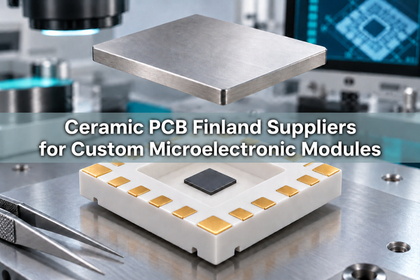
Ceramic PCB Finland projects often involve more than a flat circuit board. Selmic manufactures ceramic electronic modules, while VTT develops LTCC carriers and packaging prototypes for RF, photonics and microelectronics. At BSTCeramicPCB, we offer custom ceramic circuit fabrication in China, including multilayer and thin-film options, with component sourcing and assembly for suitable designs.
What Makes Ceramic PCB Sourcing in Finland Difficult?
The main challenge is carrying a working module design into a repeatable manufacturing process. Finland's ceramic electronics options include specialist packaging manufacture and research-led development, so the technical handover can be as important as the substrate order.
Three issues commonly arise in this type of work:
- A process-specific stack-up: An LTCC design depends on the selected ceramic tape, conductor pastes, layer thicknesses and firing process. A drawing developed for one material system may need adjustment at another manufacturer.
- Several interfaces in one module: Optical alignment, electrical connections and mechanical positioning can have separate tolerances. Passing an electrical continuity test does not verify optical coupling.
- Prototype-to-production changes: A manually assembled sample can demonstrate a concept without establishing the tooling, inspection and assembly process for repeat production.
Selmic's packaging services and VTT's development work address these integration tasks at different stages. Our fabrication service provides another route when the ceramic circuit and its manufacturing requirements are sufficiently defined for a custom board order.
Top Ceramic PCB Suppliers in Finland
Selmic and VTT are relevant Finnish sources for ceramic electronic modules, with different commercial roles. The table includes our China-based manufacturing service as an additional option for custom circuit supply.
| Supplier or development partner | Location and role | Relevant ceramic capability | Typical project stage |
|---|---|---|---|
| Mirion Technologies (Selmic) Oy | Finland; electronic-module manufacturer | Alumina and LTCC substrates, thick-film hybrids, die and wire bonding, encapsulation and testing | Module development, manufacturing and product life-cycle support |
| VTT Technical Research Centre of Finland | Finland; research and technology organization with contract manufacturing services | LTCC carriers and modules with optical, electrical and RF functions; prototyping and small-volume manufacture | Feasibility work, packaging prototypes and transfer toward industrial production |
| BSTCeramicPCB | China; custom ceramic circuit manufacturer | LTCC, HTCC, thin-film and other ceramic circuit options; component sourcing and board assembly | Custom substrate fabrication and populated-board orders |
Selmic combines ceramic substrates with module packaging. VTT is particularly relevant to a new packaging concept requiring research or pilot manufacture. We offer custom circuit production for defined electrical designs, with assembly scope agreed around the board and components.
How Do LTCC Cavities Reduce Module Height?
LTCC cavities create recessed areas within a multilayer ceramic structure. A die or component can sit below the top surface, reducing the height of the assembled module and providing space for short interconnections.
Selmic's LTCC technology includes cavities and other mechanical structures formed while the ceramic is still in its unfired state. The layers are then laminated and co-fired to create the multilayer substrate.
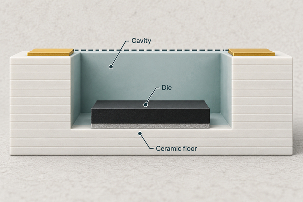
Cavity dimensions need to accommodate more than the die outline. Placement clearance, attachment material, bonding-tool access and the connection to the surrounding pads all occupy space. A cavity that fits a bare die geometrically may still leave insufficient room for assembly.
The cavity floor and adjacent layers also influence stiffness and thermal behavior. Their design is part of the ceramic stack-up, rather than a pocket added independently after the electrical layout is complete. Finished dimensions must account for the manufacturing process and its tolerances.
How Are Optical and Electrical Interfaces Integrated?
Optoelectronic modules bring light paths and electrical connections into the same package. VTT's Finnish packaging work includes LTCC-based photonics modules, where optical interfaces, high-speed circuitry and heat management must function together.
The optical path may require a fiber, lens or waveguide to align with an active device. Electrical continuity alone does not show that light is coupling efficiently. Position, angle and attachment stability can affect optical performance even when every electrical connection passes inspection.
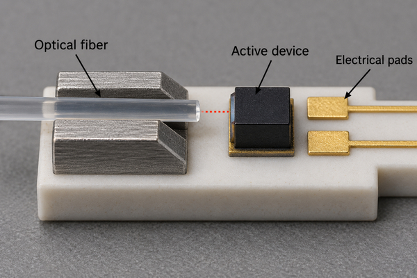
Mechanical reference features help establish the relationship between the ceramic carrier and the optical components. Their finished position matters after fabrication and after assembly. Adhesive curing or temperature changes can shift an aligned component, so the attachment process is part of the optical design.
Electrical testing and optical testing therefore answer different questions. The board can be checked for continuity and circuit function, while optical coupling or output is assessed with the appropriate optical setup. Combining the two results gives a more useful picture of module performance.
What Changes When an LTCC Prototype Moves to Production?
The production process must reproduce the prototype's electrical and mechanical behavior across repeated builds. That requires control of the ceramic material system, fired dimensions, metallization and assembly process.
LTCC tapes generally shrink during firing, with the behavior depending on the material and process. A transfer between manufacturing routes can change finished geometry unless the artwork and process settings are adapted. Nominal dimensions alone do not capture that relationship.
| Transfer item | What needs to remain controlled | Why it matters |
|---|---|---|
| Ceramic tape and conductor system | Compatible materials and qualified process conditions | Changes can affect firing, adhesion and electrical behavior |
| Finished geometry | Cavity, via and pad positions after firing | Components and interconnections must still fit |
| Assembly sequence | Attachment, bonding and any subsequent thermal steps | A later step can disturb an earlier joint or alignment |
| Test method | Reference conditions, fixtures and acceptance limits | Prototype and production results need a comparable basis |
For Finnish developers moving beyond a pilot build, the useful transfer package is the released product-and-process definition. It supports an engineering comparison between the prototype route and the proposed production route. An unchanged circuit schematic does not by itself guarantee an unchanged module.
When Does a Ceramic Module Need Hermetic Packaging?
Hermetic packaging is relevant when the internal devices need a sealed environment with a defined leakage requirement. A ceramic substrate alone does not create that enclosure: the lid, seal and electrical feedthroughs form part of the package.
A bare ceramic board, an encapsulated module and a hermetic package are different constructions. Encapsulation can protect components, but it is not automatically equivalent to a specified hermetic seal. The appropriate construction depends on the device and operating environment.
Leak testing addresses enclosure integrity. Electrical tests address circuit behavior. A finished module may require both, along with other environmental tests, but passing one does not establish the other.
Our HTCC circuit offering for satellite communication applications provides a ceramic circuit option for engineering review. The circuit's feedthrough layout and package interfaces need to match the intended enclosure. Sealing, leak testing and environmental qualification belong to the finished package's production plan.
What Advantages Does BSTCeramicPCB Offer Compared with Finnish Suppliers?
We provide a fabrication-focused supply option for custom ceramic circuits, with more than one substrate process and the choice to include board assembly. This fits projects in which the electronic design is established and specialist research or optical packaging is handled separately.
Ceramic circuit options for the electrical design
Our LTCC sensor substrate offering supports discussion of a custom multilayer sensor circuit. For a planar circuit, our thin-film board for robot-control systems uses a 1.0 mm alumina substrate. The two products represent different circuit constructions, so the process follows the design rather than a single default material stack.
Optional procurement and board assembly
We also provide ceramic PCB assembly, including component procurement, BOM checks, first-article inspection and functional testing against an agreed plan. This can combine the patterned board and its component assembly in one manufacturing order.
Selmic and VTT offer specialized integration capabilities. Our service adds a custom circuit manufacturing route in China, allowing the electrical substrate to be sourced separately from research, optical alignment or final system integration when that division suits the project.
Why Choose BSTCeramicPCB for Projects in Finland?
Choose us when a Finnish project needs a custom ceramic circuit built to a defined design, with an option to add component assembly. We align the board construction, surface finish and assembly scope with the next manufacturing operation.
For a development organization retaining its own packaging process, bare ceramic circuit supply can preserve that workflow. For an equipment manufacturer using packaged components, a populated board may provide a more convenient handover to final integration.
In Ceramic PCB Finland projects, a clear division between substrate manufacture, component assembly and specialist module operations helps keep the production route consistent. Our role is agreed around the circuit we supply, with the relevant inspections and functional tests included in the manufacturing plan.
FAQ
1. Can an LTCC cavity be added after the layer stack is finalized?
It may require changes to the stack and manufacturing process. The cavity affects available routing, layer geometry and assembly access, so it is normally considered together with the electrical layout.
2. Does every ceramic circuit need LTCC?
No. Planar thin-film, thick-film or copper-patterned ceramic circuits can be suitable when the design does not require a co-fired multilayer structure. The required connections, component layout and thermal behavior determine the choice.
3. Does a successful optical prototype prove production repeatability?
No. Repeatability also depends on fabrication tolerances, alignment, attachment and test conditions across multiple builds. A prototype proves a particular implementation; production validation checks whether the manufacturing route reproduces it consistently.
Conclusion
Finland offers strong ceramic-module development and packaging expertise through Selmic and VTT. At BSTCeramicPCB, we provide a complementary custom circuit manufacturing and assembly route from China. Contact sales@bstceramicpcb.com to discuss your ceramic board requirements.
 Products
 About us
 Contact us



