






















































 HOME


-

Aluminum Nitride Thermal Conductivity vs Temperature
2026 10,21 -
Wire Bonding EPIG Thickness: Selecting Pd/Au for Ceramic Bond Pads
2026 10,19 -
When Does a Thin-Film Circuit Need a Polished Alumina Substrate?
2026 10,18 -
Ceramic PCB for Humanoid Robot joint actuators
2026 04,07 -
LTCC PCB Surprises: What Most People Miss
2025 12,09 -
Step-by-Step Guide to DPC PCB Design for Sensor Systems
2025 12,03 -
Ceramic PCBs Essential Benefits and Applications
2025 12,01 -
How Al2O3 DPC Ceramic Substrate PCB Enhances Heat Dissipation in Modern Electronics?
2025 11,28 -
How to Choose Between Ceramic, FR4, and Metal Core PCBs
2025 11,27 -
DPC Ceramic PCB Materials: Surprising Science Inside
2025 11,26 -
Wire bondable 2-layer Alumina substrates PCB | Bstceramic PCB
2025 09,22 -
Silicon Nitride Substrate, Silicon Nitride Ceramic Substrate Formula
2025 05,08 -
What is thick film ceramic PCB?
2023 08,02
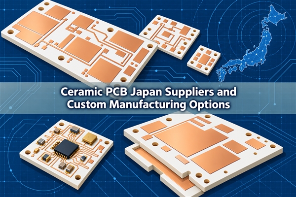
Ceramic PCB Japan Suppliers and Custom Manufacturing Options
Published:
For ceramic PCB Japan sourcing, Kansai Denshi, Kyocera, MARUWA and Noritake offer different combinations of copper-patterned boards, thin-film circuits and thick-film substrates. At BSTCeramicPCB, we supply custom ceramic PCBs from Shenzhen, with component sourcing and assembly available for customers in Japan. Our range includes DPC, DBC/DCB and AMB boards for sensor circuits, lighting and power electronics.
What Makes Ceramic PCB Sourcing in Japan Challenging?
Japan has established ceramic circuit manufacturers. The practical difficulty is matching their different technologies to a particular design, especially when developing a new board or qualifying an alternative to an existing substrate.
Different suppliers use different circuit technologies
Kansai Denshi uses its DCHC direct-copper process, Kyocera offers precision thin-film circuits, and Noritake supplies thick-film circuit substrates. These processes produce different conductor structures and follow different design rules.
For a design already built around one of these technologies, changing suppliers may require changes to conductor spacing, pad dimensions or surface finish. A circuit containing printed resistors also needs those resistor functions preserved, either within the substrate process or through a redesigned assembly. Matching the ceramic material alone does not resolve these differences.
An alternative substrate must fit the existing product
When adding a second ceramic PCB supplier to a Japanese production programme, the replacement needs to work with the existing housing, component footprints and assembly process. A change in substrate thickness can affect mounting height; a different metal finish can affect soldering or wire bonding.
An evaluation build is useful here: it allows dimensional fit and circuit operation to be checked before the new substrate enters repeat production. At BSTCeramicPCB, our manufacturing and assembly reviews address the proposed construction together, so changes to the bare board can be considered alongside their effect on component attachment.
Top Ceramic PCB Suppliers in Japan
Japan offers specialist suppliers for custom copper circuits, thin-film device carriers and printed thick-film substrates. These established suppliers specialise in different circuit technologies; their order here does not indicate market share.
Kansai Denshi Industries: custom copper-patterned ceramic boards
Kansai Denshi offers custom ceramic PCBs using alumina and aluminium nitride, with its DCHC process forming copper conductors directly on the ceramic. Its products cover development work in heat dissipation and high-frequency electronics, including lighting, communications and evaluation boards.
Small-quantity supply and standard-material stocking make it relevant to prototype programmes as well as custom board manufacture. Its custom patterns support development boards with specific pad layouts and connection positions.
Kyocera: precision thin-film circuits and ceramic packages
Kyocera offers single-layer and multilayer ceramic thin-film substrates. Its custom options include holes, steps and grooves, resistor patterns, and metallisation suited to different device-attachment requirements.
This capability is particularly relevant to laser-diode submounts, optical devices and compact electronic packages. For these products, precise device placement and the attachment surface can be central to the substrate design.
MARUWA: ceramic materials and thin-film metallisation
MARUWA combines ceramic material technology with thin-film metallisation. Its substrate range includes alumina, aluminium nitride, multilayer substrates and dielectric ceramics, with circuit products for optical communications and high-frequency applications.
The combination supports compact optical and high-frequency circuits where the substrate carries fine interconnections while removing heat from mounted devices.
Noritake: thick-film circuit substrates
Noritake supplies ceramic thick-film circuit substrates and supports pattern design through production. Its applications include automotive electronics and LED circuits. Its technical offering includes precious-metal conductors and copper-conductor systems.
Its pattern-design support is relevant when a circuit uses printed conductors and thick-film features that must be developed together on the ceramic surface.
BSTCeramicPCB: overseas ceramic PCB manufacturing and assembly
At BSTCeramicPCB, we supply DPC, DBC/DCB, AMB, thick-film, thin-film, LTCC and HTCC ceramic products. Our manufacturing operation is in Shenzhen, and our services include component sourcing and ceramic PCB assembly.
You can order a patterned bare board for your assembler in Japan, or combine fabrication and assembly with us. This gives you a choice between maintaining an existing assembly arrangement and sourcing a populated ceramic board through one supplier.
Which Ceramic PCB Materials Suit Sensor and Power Designs?
Alumina is a practical starting point for many sensor and LED circuits. Aluminium nitride is useful when heat must move quickly through a compact insulating substrate. Silicon nitride is often considered for power substrates exposed to repeated thermal and mechanical stress.
| Material | Main selection reason | Typical circuit requirement |
|---|---|---|
| Alumina (Al2O3) | Electrical insulation and a widely used base for patterned ceramic circuits | Sensor connections, LED circuits and thick-film circuitry |
| Aluminium nitride (AlN) | Higher thermal conductivity than conventional alumina grades | Compact heat-producing devices, laser submounts and power substrates |
| Silicon nitride (Si3N4) | Mechanical strength and toughness for demanding power-substrate designs | Power modules where thermal cycling stresses the ceramic and metal assembly |
Japanese suppliers offer these materials in different grades and constructions. Kansai Denshi lists alumina and AlN for ceramic boards; Kyocera and MARUWA also supply material and metallisation options for device carriers. The grade, thickness and metallisation need to be selected together. A thermal-conductivity value for the ceramic alone does not describe the thermal resistance of the assembled circuit.
For a replacement design, keeping the substrate outline while changing the ceramic can alter heat flow and expansion behaviour. We review the proposed material with the conductor layout and attachment surfaces before fabricating the replacement.
How Do DPC, DBC and AMB Ceramic PCBs Differ?
DPC forms copper circuitry by deposition and plating, DBC bonds copper to the ceramic, and AMB uses an active-metal brazing layer to join copper and ceramic. The manufacturing route affects conductor geometry, copper thickness and the materials that can be used.
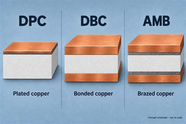
DPC ceramic PCBs suit patterned connections where pads, vias and conductor detail are central to the design. Our DPC product range includes sensor substrates; the copper pattern and finish are reviewed for the intended component connections.
DBC ceramic PCBs are used for power-device layouts with substantial copper areas. The copper provides electrical paths and heat spreading, while the ceramic provides insulation. Thick copper requires suitable separation between etched features, which can influence how closely the circuit can be routed.
AMB ceramic PCBs are another option for power substrates, including constructions using silicon nitride. The copper, brazed interfaces and ceramic form one mechanical assembly, so thermal cycling performance depends on the complete construction.
For an existing Japanese design, the original circuit process matters. Kansai Denshi's DCHC process, a Kyocera thin-film carrier and a Noritake thick-film circuit each have their own design rules. We review a proposed transfer against the selected process, including any printed resistors, fine pads or device-attachment finishes that must be retained.
Can You Order Ceramic PCB Prototypes for Evaluation in Japan?
Yes. Small-quantity ceramic board services are available from Japanese suppliers, including Kansai Denshi, and we support evaluation projects through our fabrication and assembly services. The available bare-board quantity depends on the chosen ceramic process and panel layout.
A useful prototype answers a specific product question. For a replacement substrate, that may be whether the outline and holes fit an existing housing. For a new sensor, it may be whether the pads and contacts work with the intended component arrangement. For a power board, it may be whether the assembled structure meets the project's thermal and insulation requirements.
Our design-for-manufacture and design-for-assembly reviews can address these interfaces before the prototype is built. When an evaluation leads to changes, the revised conductor pattern, finish and assembly requirements need to stay consistent for the next build. Keeping the approved construction consistent also makes prototype results more useful when moving to repeat orders.
Ceramic PCB Assembly for Projects in Japan
We can supply bare ceramic boards for assembly in Japan or provide populated boards through our ceramic PCB assembly service. The service includes component sourcing, BOM checking, solder-paste printing, placement and reflow, with inspection and testing agreed for the assembly.
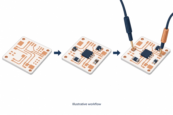
Ceramic substrates need appropriate support during handling and assembly. Their heat-transfer characteristics also affect the temperature profile at the solder joints. Pad finish, component termination and soldering conditions therefore need to be considered together. We review these requirements with the board construction before production.
Our inspection capabilities include solder-paste inspection, optical inspection and X-ray inspection. Optical inspection checks visible assembly features; X-ray inspection can examine suitable hidden solder connections. Functional testing checks the circuit against the agreed test requirements. These methods serve different purposes and are selected for the actual assembly.
If you keep your current assembler in Japan, we can supply the patterned substrate to its specified finish and geometry. If you source the populated board from us, you can receive it for the next stage of equipment integration or product evaluation.
What Affects Ceramic PCB Cost and Delivery to Japan?
Material, circuit process, usable panel area, conductor detail and assembly content all affect ceramic PCB cost. A compact alumina sensor board and a heavy-copper AlN power substrate require different materials and manufacturing operations, even if their outer dimensions are similar.
For prototypes, setup and tooling costs are shared across a small quantity. For repeat orders, panel utilisation and a stable construction become more significant. Using an available standard thickness can simplify material preparation, provided it meets the mechanical and thermal design requirements.
When comparing supply in Japan with shipment from Shenzhen, compare the delivered total for the same construction. That includes the boards, any component sourcing and assembly, freight, clearance charges and applicable import taxes. Bare boards and populated assemblies should be described accurately for customs handling; the importer or broker confirms the classification and charges for the shipment.
Japanese import clearance generally uses an invoice and transport documentation, with a packing list and other supporting documents as required. Clear descriptions, quantities and values help the receiving party prepare the entry. We coordinate production and shipping arrangements with the order so that the arrival plan supports your assembly or evaluation schedule in Japan.
What Advantages Does BSTCeramicPCB Offer Compared with Japanese Suppliers?
Our main advantages are a choice of ceramic circuit processes and the ability to combine board fabrication with component sourcing and assembly. You can compare several substrate options with us while keeping the finished circuit requirements in the same discussion.
| Project requirement | Relevant Japanese supply options | What we offer |
|---|---|---|
| Custom copper-patterned ceramic board | Kansai Denshi's DCHC ceramic PCBs | DPC, DBC/DCB and AMB product options for different conductor and substrate requirements |
| Precision thin-film circuit or device carrier | Kyocera and MARUWA thin-film substrates | Thin-film ceramic products alongside other ceramic circuit families, with the construction reviewed for the application |
| Printed thick-film circuitry | Noritake thick-film circuit substrates | Thick-film ceramic PCB supply within our wider ceramic board offering |
| A populated ceramic board | Japanese substrate suppliers can be combined with the project's selected assembler | Fabrication, component sourcing and assembly available through BSTCeramicPCB |
The combined service is useful when an assembly decision changes the board itself. For example, a revised component may need a different pad geometry or finish. We can review that change against both fabrication and assembly requirements before committing the revised board to production.
We also provide an alternative manufacturing source for an existing design. A second source can give your purchasing programme another supply option once the replacement has completed your approval process. We review the replacement against the required outline, conductor pattern and assembly interfaces, then support an evaluation build for your product approval.
Why Choose BSTCeramicPCB for Your Ceramic PCB Project in Japan?
BSTCeramicPCB is a practical choice when your project needs a custom patterned substrate, manufacturing input during development and a route to an assembled board. Our sensor and power-substrate products provide concrete starting points for that work.
Developing a sensor board for evaluation
Our DPC ceramic sensor substrate provides a concrete example: 96% alumina with 35 micrometre copper. For a sensor-board project, the ceramic outline, contact positions and conductor pattern can be reviewed against the intended mechanical and electrical arrangement.
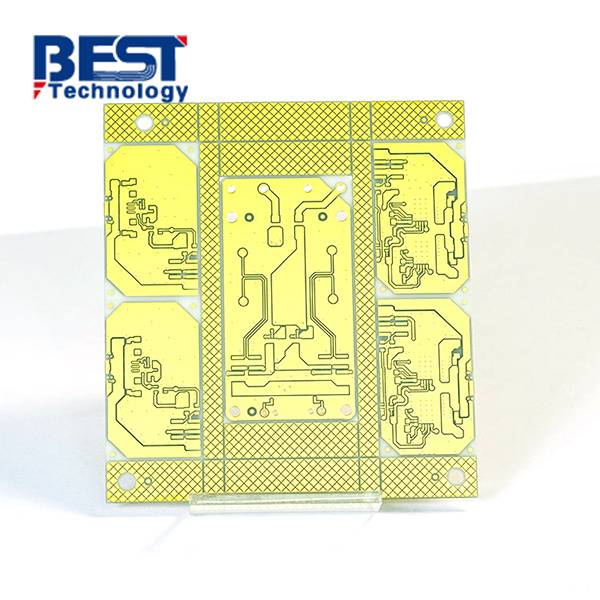
If you need populated evaluation boards, our assembly service includes BOM checking and first-article inspection. This allows the initial build to be checked before it is used for your sensor or equipment evaluation in Japan.
Sourcing a substrate for a power-device layout
Our DBC substrate for IGBT applications uses aluminium nitride with 300 micrometre copper. We also supply double-sided AMB ceramic PCBs. These are relevant options when the design requires substantial copper paths and heat transfer through an electrically insulating ceramic.
For a custom AlN board with 300 micrometre copper, we review the conductor layout, device-attachment areas and mounting arrangement together. This is particularly useful when the substrate must fit an existing power-module layout.
Keeping a development project with one manufacturing contact
A project may begin with bare substrates and later need populated samples. We can support that transition with board manufacture, component sourcing and assembly under the same supply relationship. For a Japanese equipment developer, the benefit is continuity between the circuit pattern being evaluated and the board that reaches assembly.
FAQ
1. Is DCHC the same as DPC?
DCHC is Kansai Denshi's named ceramic circuit process. DPC refers to direct plated copper technology. Both involve copper circuitry on ceramic, but their process details and design rules should be checked separately when transferring a design.
2. Can a ceramic PCB include printed resistors?
Yes. Resistor patterns are available in some thin-film and thick-film technologies. Their resistance, tolerance and trimming requirements belong in the circuit design. They are not automatically included in a standard DPC, DBC or AMB board.
3. Can I reuse an existing ceramic PCB layout with a new supplier?
The layout can be the starting point, but the new manufacturing process may require changes to spacing, pads, holes or finishes. An evaluation build should check the revised substrate in the intended assembly before production approval.
Conclusion
For ceramic PCB Japan projects, BSTCeramicPCB offers custom bare-board manufacture and the option of component sourcing and assembly. If you are developing a sensor circuit, sourcing a power substrate or evaluating an additional manufacturer, contact sales@bstceramicpcb.com to discuss the construction.
 Products
 About us
 Contact us



