






















































 HOME


-

Aluminum Nitride Thermal Conductivity vs Temperature
2026 10,21 -
Wire Bonding EPIG Thickness: Selecting Pd/Au for Ceramic Bond Pads
2026 10,19 -
When Does a Thin-Film Circuit Need a Polished Alumina Substrate?
2026 10,18 -
Ceramic PCB for Humanoid Robot joint actuators
2026 04,07 -
LTCC PCB Surprises: What Most People Miss
2025 12,09 -
Step-by-Step Guide to DPC PCB Design for Sensor Systems
2025 12,03 -
Ceramic PCBs Essential Benefits and Applications
2025 12,01 -
How Al2O3 DPC Ceramic Substrate PCB Enhances Heat Dissipation in Modern Electronics?
2025 11,28 -
How to Choose Between Ceramic, FR4, and Metal Core PCBs
2025 11,27 -
DPC Ceramic PCB Materials: Surprising Science Inside
2025 11,26 -
Wire bondable 2-layer Alumina substrates PCB | Bstceramic PCB
2025 09,22 -
Silicon Nitride Substrate, Silicon Nitride Ceramic Substrate Formula
2025 05,08 -
What is thick film ceramic PCB?
2023 08,02
Ceramic PCB Korea Suppliers for Power and RF Projects
Published:
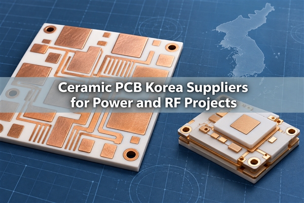
Ceramic PCB Korea suppliers offer several distinct technologies: KCC produces DCB and AMB power substrates, RN2 Ceramics develops printed-copper ceramic substrates, and AMOSENSE manufactures LTCC products for RF and other electronic applications. At BSTCeramicPCB, we are a ceramic PCB supplier in China providing custom substrates, component sourcing and assembly. Our DBC/DCB, AMB and LTCC options give Korean customers a choice between a bare ceramic circuit and a combined fabrication-and-assembly order.
What Makes Ceramic PCB Sourcing in Korea Difficult?
The main challenge is matching the circuit to a supplier's manufacturing process. Korea has suppliers working on thick copper power substrates, printed copper structures and multilayer RF ceramics. These products differ in conductor geometry, internal connections and assembly requirements.
- Changing the copper process can change the module. A power design with copper at several heights cannot move directly to a uniform-thickness copper sheet without changing its mechanical interfaces.
- An RF layout is tied to its ceramic stack-up. Layer thickness, dielectric properties and via geometry affect impedance and frequency response. Moving an LTCC design to another material system can require a new simulation and prototype.
- Prototype and production costs have different drivers. Screens, tooling, layer preparation and test fixtures are spread over fewer units in a small run. A board's area alone does not explain its prototype price.
- A substrate and a finished module are different orders. Die attachment, surface-mount assembly and RF characterization add operations beyond ceramic fabrication. The required delivery stage affects the supplier shortlist.
For projects keeping assembly in Korea, we can supply custom bare ceramic PCBs. For projects combining fabrication and population, our ceramic PCB assembly service brings the board and component work into one order.
Top Ceramic PCB Suppliers in Korea
KCC, RN2 and AMOSENSE cover different parts of Korea's ceramic electronics supply chain. The comparison below also includes BSTCeramicPCB as a manufacturing option in China.
| Supplier | Location and role | Relevant products and capabilities | Suitable projects |
|---|---|---|---|
| KCC | Korea; ceramic materials and substrate manufacturer | DCB and AMB ceramic power substrates, including alumina and aluminum nitride options | Power modules requiring copper-clad ceramic substrates |
| RN2 Technologies / RN2 Ceramics | Korea; ceramic electronic components and substrates | LTCC technology and TPC printed-copper substrates, including structures with different copper heights | RF ceramic components and power-module designs using printed copper |
| AMOSENSE | Korea; ceramic materials and electronic modules | LTCC antenna-in-package products, multilayer ceramic structures and silicon nitride ceramic products | Integrated RF packaging, antennas and ceramic module development |
| BSTCeramicPCB | China; custom ceramic PCB supplier | DBC/DCB, AMB and LTCC products, custom fabrication, component sourcing and ceramic PCB assembly | Custom bare substrates or fabrication-and-assembly projects |
For a power module built around bonded copper, KCC's DCB/AMB range is directly relevant. RN2's printed-copper structures address a different conductor construction, while AMOSENSE's LTCC antenna products combine RF functions within a ceramic package. We serve projects requiring a custom ceramic circuit with a separately defined fabrication or assembly scope.
What Is a TPC Ceramic Substrate?
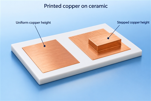
TPC stands for Thick Printing Copper. RN2 Ceramics uses screen printing to form copper patterns on ceramic substrates such as alumina, zirconia-toughened alumina and aluminum nitride. Successive printing steps can produce different conductor heights on the same substrate.
That construction is useful when a power module needs a raised contact or copper spacer as part of the substrate. The height becomes a mechanical feature, alongside the copper pattern's electrical function. RN2 also offers individual circuit substrates and larger mastercards for subsequent processing.
TPC differs from DBC, where copper foil is bonded to ceramic, and from AMB, where an active braze joins the copper and ceramic. A transfer between these processes therefore involves more than matching the top-view artwork. Contact height, copper cross-section and the connection to the cooling assembly may also change.
When Does an RF Project Need LTCC?
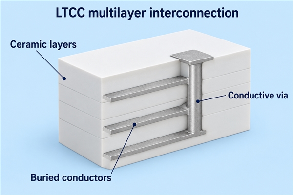
LTCC is useful when an RF circuit needs buried interconnections, compact multilayer routing or integrated passive structures. Conductive patterns and vias are formed within ceramic layers that are co-fired into one structure.
AMOSENSE's LTCC antenna-in-package products illustrate this approach in Korea. Its 28 GHz product combines an RF module and antenna, and its LTCC technology accommodates an embedded RF power divider. This is a different design task from putting large copper pads on a ceramic power substrate.
For a custom RF ceramic substrate PCB, the material system and layer geometry influence the circuit together. A change in dielectric constant alters electrical length; a change in via or ground layout can affect the transition between layers. RF validation consequently follows the finished stack-up and operating band.
We offer LTCC ceramic substrates for power-amplifier projects. Custom layer structures and metallization require engineering review. The substrate design, semiconductor selection and complete amplifier performance remain separate parts of the development work.
What Affects Ceramic PCB Prototype Cost?
Ceramic PCB prototype cost is driven by the manufacturing route, setup work, usable panel area and verification scope. In Korea's power-substrate and LTCC supply market, two boards with similar outer dimensions can require very different production steps.
| Cost factor | Power-substrate example | LTCC example |
|---|---|---|
| Material and construction | Ceramic grade, ceramic thickness and copper thickness | Ceramic tape system, layer count and fired thickness |
| Pattern preparation | Copper geometry, edge clearances and machining | A separate pattern for each conductor layer, plus via preparation |
| Panel utilization | Board outline and spacing between circuits | Layout repeated within the usable co-firing area |
| Assembly | Component attachment and thermal interfaces | Surface components, package connections and RF transitions |
| Verification | Insulation, dimensions and attachment quality | Continuity, layer registration and frequency-dependent measurements |
For small batches, fixed setup costs can outweigh the material saving from a slightly smaller board. Reusing an approved construction across revisions can reduce repeated preparation, provided the electrical and mechanical requirements stay compatible. Assembly and specialized testing also need to be included when comparing the cost of a completed circuit rather than a bare substrate.
What Advantages Does BSTCeramicPCB Offer Compared with Korean Suppliers?
Our strengths are custom ceramic PCB fabrication across several process families and the option to combine that work with component sourcing and assembly. For a Korean project requiring its own circuit layout, this provides a practical alternative to purchasing a substrate or integrated module from a specialist product range.
Power-substrate options for custom layouts
Our AlN DBC substrate for IGBT applications uses 300 micrometre copper. We also supply double-sided AMB ceramic PCBs. These give a power project concrete starting points for reviewing copper layout, ceramic thickness and attachment surfaces. A custom construction is confirmed against the circuit and assembly requirements.
Fabrication and assembly in one order
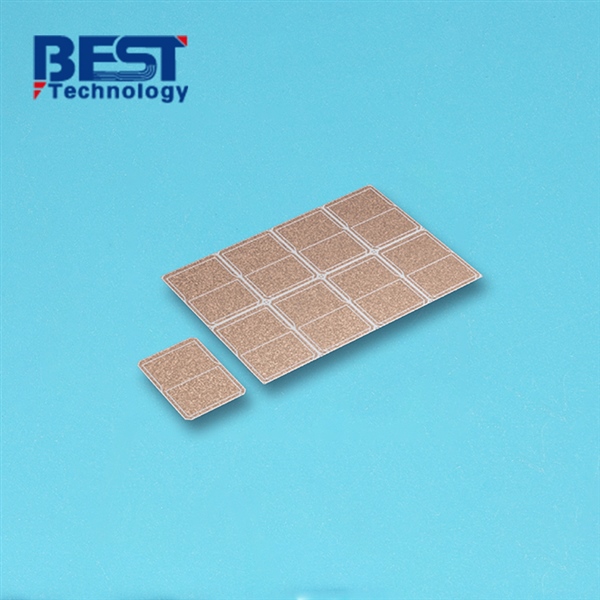
Our ceramic PCB assembly service includes component sourcing, manufacturability and assembly reviews, first-article work and functional testing within the agreed project scope. Coordinating these stages lets us address pad finish, component placement and board handling before the bare boards reach assembly.
Support for both power and multilayer circuit development
Our DBC/DCB and AMB products support copper-patterned power circuits, while our LTCC range serves multilayer ceramic projects. A company developing separate power and signal modules can discuss both substrate requirements with us. Each circuit retains its own material, layout and validation requirements.
Compared with the Korean suppliers above, our offer is particularly relevant when the required output is a custom board or assembled circuit rather than a specific antenna package or printed-copper module structure. We can supply the bare substrate for an existing assembly line or include population in the project.
How Are Power and RF Ceramic Circuits Tested?
Power and RF ceramic circuits require different electrical checks because their operating stresses differ. Power-substrate verification concentrates on insulation and the thermal-mechanical construction; RF verification also examines signal behavior across the intended frequency band.
For a DCB, AMB or TPC power substrate, dimensional inspection covers the ceramic outline, copper pattern and critical contact surfaces. Insulation resistance and dielectric withstand checks address electrical separation under specified conditions. Thermal cycling evaluates the effect of repeated expansion and contraction on the ceramic-to-metal structure. The voltage, duration and temperature profile must match the approved qualification plan.
For an LTCC RF circuit, continuity testing checks connections but does not establish RF performance. Measurements such as insertion loss and return loss evaluate transmission and reflections across frequency. The test fixture and transitions contribute to the measurement, so comparison between prototypes needs a consistent setup.
For assembled boards, inspection and functional testing address the populated circuit. At BSTCeramicPCB, we agree the assembly test scope with the project requirements; a standard continuity check and a complete RF characterization are different services.
Why Choose BSTCeramicPCB for Ceramic PCB Projects in Korea?
Choose BSTCeramicPCB when your project needs a custom ceramic circuit and a clear path from prototype fabrication to the required delivery stage. We are based in China and work with Korean customers on bare-board and assembly requirements.
For a power prototype, we can review a DBC or AMB construction around the intended copper pattern and component attachment. When the design moves to an assembled prototype, we can add sourcing and assembly to the order. If your production line already handles population in Korea, the order can remain a bare-board supply arrangement.
For a multilayer RF project, we can review the ceramic stack-up and interconnections for a custom LTCC substrate. Your RF development work can then proceed with the selected substrate construction, followed by measurements on the assembled circuit.
This flexibility is useful when different development stages need different deliverables: an unpopulated substrate for mechanical trials, a populated board for functional evaluation, or repeat fabrication of an approved circuit.
FAQ
1. Are DCB and DBC ceramic substrates different technologies?
DCB and DBC commonly refer to the same direct copper bonding process. The abbreviations alone do not define a different product. Ceramic grade, copper thickness, pattern geometry and finish distinguish individual constructions.
2. Is an LTCC substrate the same as a ceramic antenna?
No. LTCC is a multilayer ceramic manufacturing technology. It can be used to build antenna-in-package structures, but it also supports other circuits and packages. A discrete ceramic antenna is a component with its own frequency and mounting requirements.
3. Can one ceramic PCB material replace another without changing the design?
Not automatically. A power circuit may be affected by changes in thermal conductivity, expansion and mechanical strength. An RF circuit may also be affected by dielectric constant and loss. The replacement requires evaluation using the new material's properties and the actual circuit construction.
Conclusion
Ceramic PCB Korea sourcing spans bonded-copper power substrates, printed-copper structures and multilayer RF ceramics. BSTCeramicPCB offers custom fabrication in China with the option to include component sourcing and assembly. Contact sales@bstceramicpcb.com to discuss a ceramic circuit for your next project.
 Products
 About us
 Contact us



