






















































 HOME


-

Aluminum Nitride Thermal Conductivity vs Temperature
2026 10,21 -
Wire Bonding EPIG Thickness: Selecting Pd/Au for Ceramic Bond Pads
2026 10,19 -
When Does a Thin-Film Circuit Need a Polished Alumina Substrate?
2026 10,18 -
Ceramic PCB for Humanoid Robot joint actuators
2026 04,07 -
LTCC PCB Surprises: What Most People Miss
2025 12,09 -
Step-by-Step Guide to DPC PCB Design for Sensor Systems
2025 12,03 -
Ceramic PCBs Essential Benefits and Applications
2025 12,01 -
How Al2O3 DPC Ceramic Substrate PCB Enhances Heat Dissipation in Modern Electronics?
2025 11,28 -
How to Choose Between Ceramic, FR4, and Metal Core PCBs
2025 11,27 -
DPC Ceramic PCB Materials: Surprising Science Inside
2025 11,26 -
Wire bondable 2-layer Alumina substrates PCB | Bstceramic PCB
2025 09,22 -
Silicon Nitride Substrate, Silicon Nitride Ceramic Substrate Formula
2025 05,08 -
What is thick film ceramic PCB?
2023 08,02
Ceramic PCB Taiwan Suppliers for LED and Laser Modules
Published:
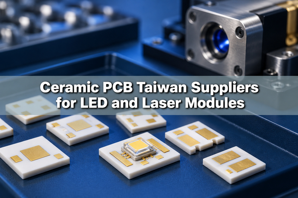
Ceramic PCB Taiwan suppliers serve several stages of electronic packaging, from precision alumina sheets to patterned ceramic circuits. Tong Hsing supplies metallized substrates, LEATEC manufactures precision ceramic substrates, and Regulus coordinates ceramic board fabrication through manufacturing partners. At BSTCeramicPCB, we manufacture custom ceramic circuits in China, including DPC boards for LED and laser applications, with component sourcing and assembly available for suitable designs.
What Makes Ceramic PCB Sourcing in Taiwan Difficult?
The main difficulty is matching a supplier's product to the required stage of the package build. An unpatterned alumina sheet, a metallized LED submount and an assembled laser-control board are different deliverables, even when all three use a ceramic substrate.
Taiwan's ceramic supply options include both material specialists and circuit manufacturers. A packaging project can therefore involve several interfaces: the ceramic dimensions, deposited metal stack, die attachment and final separation into individual parts.
- Small pad geometry: The metal pattern must accommodate the die, external connections and electrical isolation within a limited area.
- Panel-to-part consistency: Circuit placement and the cutting layout must leave enough clearance around the finished part. Edge damage can affect a small submount disproportionately.
- Thermal interfaces: A high-conductivity substrate cannot compensate for a poorly formed joint beneath the die or beneath the ceramic.
- Supply scope: A ceramic material order does not include circuit patterning unless that work is part of the agreed product. Assembly adds another set of process requirements.
Our custom fabrication service covers the patterned circuit. For populated boards, we also review component attachment and testing as part of the assembly scope.
Top Ceramic PCB Suppliers in Taiwan
The following suppliers cover different parts of Taiwan's ceramic electronics supply chain. Their roles are useful distinctions when comparing a ceramic material order with a completed circuit order.
| Supplier | Supply role | Relevant capabilities | Suitable project scope |
|---|---|---|---|
| Tong Hsing Electronic Industries | Metallized ceramic substrate manufacturer in Taiwan | DPC using sputtering and photolithography; applications include LEDs, RF, laser systems and semiconductor equipment | Patterned ceramic substrates for electronic packaging |
| LEATEC Fine Ceramics | Precision ceramic substrate manufacturer in Taiwan | Alumina substrates for resistor products, hybrid ICs, LED packaging and sensing applications | Ceramic substrate materials and application-specific ceramic parts |
| Regulus | Taiwan-based engineering and supply coordinator | Alumina and AlN ceramic boards, with thin-film and thick-film fabrication through qualified manufacturing partners | Projects combining engineering support with coordinated board sourcing |
| BSTCeramicPCB | Custom ceramic circuit manufacturer in China | DPC and other ceramic circuit processes, component sourcing and PCB assembly | Custom boards supplied bare or populated |
Tong Hsing's DPC offering is directly relevant to metallized packaging substrates. LEATEC's focus starts with precision ceramic materials. Regulus provides a coordinated sourcing service. We offer custom circuit fabrication with the option to include assembly, so the order can follow the needs of the finished electronic design.
Why Is DPC Used for LED and Laser Submounts?
DPC provides patterned copper connections on an electrically insulating ceramic base. That combination suits compact optoelectronic assemblies where the substrate must carry current and transfer heat away from a small active area.
Tong Hsing identifies high-power LEDs and laser systems among its DPC applications. The process uses deposited seed layers and photolithographic patterning before building the copper circuit. The resulting pad layout can separate electrical connections while placing a heat-spreading metal area beneath or near the device.
Our alumina DPC board for LED chips uses a 1.0 mm alumina substrate and 18 μm copper. It is one example of a ceramic PCB substrate configured for an LED application. The copper thickness and ceramic thickness for another package need to follow its electrical, thermal and assembly requirements.
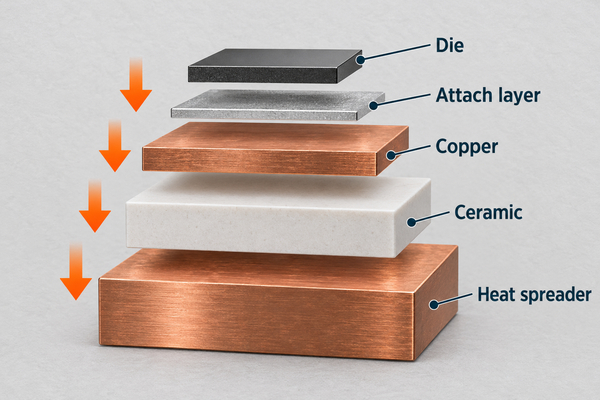
The package layout also determines how heat spreads beyond the die footprint. A larger metal area can distribute heat into more ceramic, but adjacent isolated pads and available package space limit that area. Substrate selection and circuit geometry therefore need to be evaluated together.
How Do Thermal Vias Help a Ceramic Package?
Metallized vias can connect the two faces of a ceramic circuit and provide an additional heat-conduction path where the design and fabrication process support them. They can also route an electrical connection from a top-side pad to a bottom-side terminal.
Ceramic itself conducts heat through the substrate, unlike a conventional low-conductivity polymer dielectric. A via is therefore not automatically required beneath every device. Its benefit depends on the ceramic material, hole construction, copper distribution and the thermal interface beneath the board.
An electrically connected via also changes the net connectivity. A top-side power pad linked to bottom copper cannot share that copper with an isolated signal without a short circuit. In an LED or laser package, the electrical net assignment must remain consistent with the intended thermal arrangement.
Filled and plated-wall vias are different structures. Their dimensions and process limits need to be established for the selected ceramic construction; FR-4 via rules cannot simply be copied into a ceramic package drawing.
What Determines Ceramic Substrate Panel Size?
Panel size is determined by the fabrication process, circuit arrangement and separation method. For small LED or sensor parts, the production panel also provides room for handling and alignment before the individual circuits are separated.
The panel layout includes more than the saleable circuit area. Cutting streets, tooling space and edge clearances reduce the number of usable parts. Placing a copper pad too close to a cut can leave an inadequate margin on the finished ceramic, even if the panel artwork appears to fit.
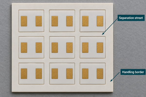
| Panel feature | Purpose | Effect on the finished part |
|---|---|---|
| Separation street | Space for the chosen cutting process | Sets the gap between neighboring circuit outlines |
| Metal-to-edge clearance | Keeps functional metal away from the cut edge | Reduces the chance that edge damage reaches a pad or trace |
| Alignment features | Locate the panel during processing or assembly | Establish the reference used for pad and component placement |
| Handling area | Allows gripping or supporting the panel | Keeps handling loads away from small finished circuits |
The agreed deliverable may be a panel or separated parts. This affects assembly fixtures and handling downstream, so it should remain consistent from prototype evaluation into repeat orders.
How Does Die Attachment Affect Heat Flow?
The layer beneath a die can contribute substantial thermal resistance. Its thickness, conductivity and contact area affect how efficiently heat enters the ceramic circuit.
A void interrupts contact in part of the joint. Its location matters: a void beneath the hottest area can have a different effect from one near an unloaded edge. Evaluating the complete heat path includes the die joint, patterned metal, ceramic and board-to-heatsink interface.
Solder, sintered materials and conductive adhesives also have different processing requirements. Their suitability depends on the die metallization, substrate finish and operating conditions. Changing the attachment material can require a different thermal cycle or surface preparation.
For a packaged LED mounted by SMT, the component manufacturer has already defined much of the internal die-attachment structure. The board assembly then controls the external solder joint. For bare-die packaging, attachment and interconnection require a separately defined packaging process.
What Advantages Does BSTCeramicPCB Offer Compared with Taiwan Suppliers?
We offer a custom circuit supply route with concrete DPC constructions and optional assembly. This is useful when the requirement is a board built to an existing layout rather than an unpatterned ceramic sheet or a complete semiconductor package.
Copper layouts tailored to the circuit
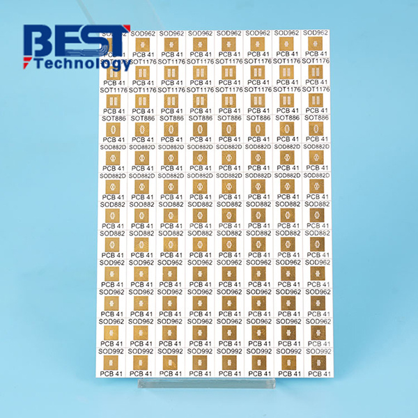
Our double-sided DPC board for laser equipment uses 96% alumina with 70 μm top copper and 35 μm bottom copper. Our DPC board for cooling equipment combines 35 μm copper with 200 μm copper in a specified area. These examples show different copper arrangements for different circuit tasks; they are not interchangeable specifications for every design.
Fabrication with a choice of delivery stage
We can supply the patterned board for assembly by an existing partner. We can also combine fabrication with component procurement and ceramic PCB assembly, including first-article inspection and functional testing to an agreed plan.
For projects in Taiwan, we can deliver the patterned ceramic to an existing packaging partner or supply a populated board for equipment integration. The agreed scope links the copper construction, surface finish and assembly requirements in one production plan.
Why Choose BSTCeramicPCB for Projects in Taiwan?
Choose us for custom ceramic boards when the electrical layout is established and the project needs a practical path from fabricated substrate to board assembly. We support LED, laser and sensor circuit work without treating each application as the same standard board.
A packaging developer may retain die bonding and optical alignment with its specialist partner while sourcing the patterned ceramic separately. An equipment manufacturer using packaged components may instead prefer a populated board. These two workflows have different responsibilities, and our supply scope can be defined around the required board stage.
For Ceramic PCB Taiwan projects, we review the proposed ceramic construction and assembly requirements before production. That review helps align the delivered board with the next operation, whether it is local packaging, SMT assembly or integration into the instrument.
FAQ
1. Is a ceramic substrate always supplied with copper tracks?
No. Precision ceramic sheets may be supplied without a circuit pattern. A metallized substrate adds conductive layers and defined connections. The product specification determines which stage is supplied.
2. Does thicker copper always improve an LED substrate?
Thicker copper can help current carrying and heat spreading, but it also affects patterning and assembly geometry. The required trace width, isolation gap and component attachment determine an appropriate construction.
3. Can an LED ceramic board also be used for a laser module?
Only if its electrical layout, thermal path and mechanical interfaces meet that module's requirements. A similar ceramic material does not make the pad layout or package dimensions interchangeable.
Conclusion
Taiwan's ceramic supply chain includes precision substrate materials, metallized packaging circuits and coordinated fabrication services. At BSTCeramicPCB, we offer custom ceramic board manufacturing in China with optional component sourcing and assembly. Contact sales@bstceramicpcb.com to discuss your circuit application.
 Products
 About us
 Contact us



