






















































 HOME
HOME

-

Ceramic PCB for Humanoid Robot joint actuators
2026 04,07 -
LTCC PCB Surprises: What Most People Miss
2025 12,09 -
Step-by-Step Guide to DPC PCB Design for Sensor Systems
2025 12,03 -
Ceramic PCBs Essential Benefits and Applications
2025 12,01 -
How Al2O3 DPC Ceramic Substrate PCB Enhances Heat Dissipation in Modern Electronics?
2025 11,28 -
How to Choose Between Ceramic, FR4, and Metal Core PCBs
2025 11,27 -
DPC Ceramic PCB Materials: Surprising Science Inside
2025 11,26 -
Wire bondable 2-layer Alumina substrates PCB | Bstceramic PCB
2025 09,22 -
Silicon Nitride Substrate, Silicon Nitride Ceramic Substrate Formula
2025 05,08 -
What is thick film ceramic PCB?
2023 08,02
Alumina Structure: Crystal Phases, Properties and PCB Use
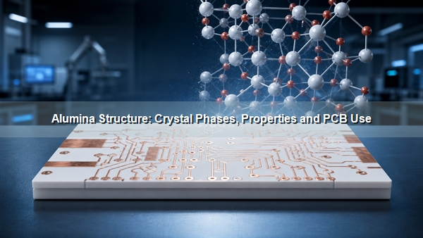
Alumina structure describes how aluminum and oxygen ions are arranged in Al2O3 and how real ceramic grains, pores, and secondary phases form a substrate. Dense ceramic PCB grades are predominantly alpha-alumina, the stable corundum phase. Its crystal network supports high electrical insulation, hardness, chemical stability, and dimensional stability, but finished-substrate behavior still depends on purity, porosity, grain size, surface condition, and metallization.
What Is the Structure of Alumina?
Alumina is aluminum oxide, Al2O3, and its solid form is an extended crystal lattice rather than a collection of isolated Al2O3 molecules. The most stable form is alpha-alumina, also called corundum. In dense electronic substrates, this phase is the main structural framework that carries mechanical load and separates conductive circuit features.
Commercial alumina ceramics are polycrystalline. Each grain has the alpha-alumina crystal structure, while grain boundaries may contain small amounts of additives or glassy phases introduced to control sintering. That distinction matters: the ideal crystal explains the intrinsic material behavior, but the microstructure controls many properties measured on an actual PCB substrate.
How Are Aluminum and Oxygen Ions Arranged in Alpha-Al2O3?
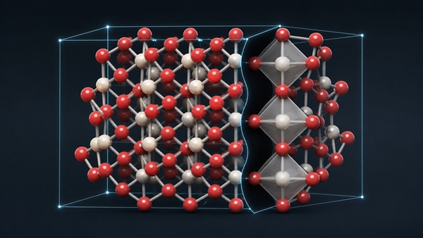
In alpha-Al2O3, oxygen ions form a close-packed framework and aluminum ions occupy two-thirds of the available octahedral sites. Each aluminum ion is coordinated by six oxygen ions. The crystal is commonly described with the trigonal corundum structure and space group R-3c.
This ordered three-dimensional network has strong mixed ionic and covalent bonding. It leaves very few mobile charge carriers at normal operating temperatures, which is one reason dense alumina is an effective electrical insulator. The same tightly bonded structure also resists indentation and wear.
Alpha, Gamma, Delta and Theta Alumina Structures
Alpha-alumina is the thermodynamically stable phase used for dense structural and electronic ceramics. Gamma, delta, and theta alumina are transition phases that can form during powder processing and heat treatment before conversion to alpha-alumina.
| Alumina phase | General structural character | Typical relevance |
|---|---|---|
| Alpha (α) | Dense corundum structure | Ceramic substrates, wear parts, insulators |
| Gamma (γ) | Defective spinel-like transition structure with high surface area | Catalysts and adsorbents |
| Delta (δ) | Transitional ordered structures | Intermediate during thermal transformation |
| Theta (θ) | Transitional monoclinic-related structure | Intermediate before alpha conversion |
PCB substrates require a dense, low-porosity body rather than the high-surface-area behavior valued in catalyst supports. The firing schedule and starting powder are therefore controlled to develop the intended alpha-alumina microstructure.
How Does Alumina Structure Create Electrical Insulation?
The alumina lattice binds electrons strongly, so bulk electrical resistivity is high when the material is dense, clean, and used within its temperature and voltage limits. For example, one published 99% alumina grade lists volume resistivity above 10^14 Ω·cm at 20°C; that value belongs to that grade and test condition, not to every alumina substrate.
Electrical isolation can still be reduced by surface contamination, moisture films, pores, conductive residues, high temperature, or an electric field concentrated at a sharp metal edge. A ceramic PCB design must therefore combine suitable substrate material with adequate creepage, clearance, metallization spacing, and cleaning.
How Does Alumina Structure Affect Heat Flow and Hardness?
The continuous crystal network transfers heat more effectively than many polymeric PCB dielectrics, while its strong bonding produces high hardness and wear resistance. Heat flow is limited by anything that scatters phonons, including pores, impurities, glassy grain-boundary phases, and microcracks. Higher purity and density often improve thermal performance, but the actual datasheet must be used.
Hardness is not the same as fracture toughness. Alumina can resist scratching and indentation yet still chip if a thin edge, drilled hole, or mounting point experiences a concentrated tensile load. Designers should treat hardness, flexural strength, fracture toughness, elastic modulus, and edge quality as separate inputs.
Why Do Purity, Porosity and Grain Size Matter?
Purity, porosity, and grain size determine how closely a fired ceramic approaches ideal alpha-alumina behavior. Lower-purity grades use more sintering aids or glassy phases, which can reduce firing temperature and cost but may change thermal conductivity, dielectric loss, strength, and chemical resistance.
Open pores can hold contaminants and create weak paths. Closed pores reduce the load-bearing and heat-conducting cross-section. Grain size and grain-boundary chemistry influence strength, surface finish, metallization adhesion, and the stability of small features. For this reason, a 96% Al2O3 DPC ceramic substrate PCB for sensors must be evaluated with its actual substrate specification rather than a generic value for high-purity alumina.
For density terminology and grade-to-grade variation, see the BSTCeramicPCB guides to alumina density and different grades of alumina.
How Does Sintering Build a Dense Alumina Substrate?
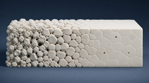
Sintering bonds compacted alumina particles into a coherent polycrystalline body. Powder composition, particle-size distribution, forming pressure, binder removal, peak temperature, and dwell time all affect shrinkage, pore removal, grain growth, flatness, and final density.
The ceramic must shrink predictably so that finished holes, outlines, and metallized features meet tolerance. Excessive grain growth can reduce strength consistency, while incomplete densification leaves residual porosity. The manufacturing route described in how to make an alumina PCB should therefore be matched to the required purity, thickness, surface finish, and circuit process.
Why Does Alumina Structure Matter for Metallization?
Metallization adheres to a real ceramic surface, not to an ideal lattice. Surface roughness, cleanliness, porosity, grain boundaries, and any glassy phase affect activation, deposition, printing, firing, brazing, and copper bonding. The suitable interface is different for thick-film, thin-film, DPC, DBC, and co-fired processes.
A fine-feature alumina DPC ceramic substrate PCB for LED applications uses a different metal-building process from a 96% Al2O3 thick-film ceramic substrate PCB. Their base chemistry may be similar, but conductor thickness, interface formation, line geometry, adhesion mechanism, and thermal stress are not interchangeable. See ceramic PCB metallization processes for the process comparison.
How Does Alumina Structure Affect Cutting, Holes and Edges?
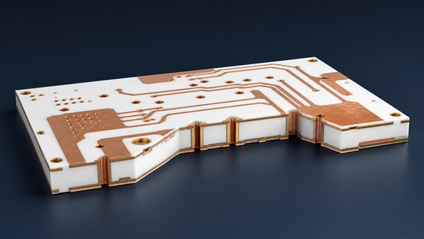
The hard, brittle alumina microstructure requires controlled laser cutting, drilling, scribing, grinding, or dicing. A process that removes material efficiently can still introduce a heat-affected zone, microcracks, recast material, edge chips, or residual stress.
Feature size should be reviewed together with substrate thickness, purity, hole-to-edge distance, corner radius, panelization method, and final load path. Rounded internal corners, realistic edge clearances, and inspection of critical holes reduce the chance that a local flaw becomes the origin of a crack. The BSTCeramicPCB guide to cutting alumina ceramic substrates covers these manufacturing considerations in more detail.
Which Alumina Grade Fits a Ceramic PCB?
The right grade is the one whose verified electrical, thermal, mechanical, surface, and manufacturing properties satisfy the application together. A higher alumina percentage may improve selected properties, but it can also change sintering behavior, machining cost, surface finish, and metallization compatibility.
Review these items before locking the substrate:
- alumina content and secondary phases;
- thermal conductivity and operating temperature;
- volume and surface resistivity, dielectric strength, and dielectric loss;
- flexural strength, fracture toughness, hardness, and elastic modulus;
- thickness, flatness, roughness, and dimensional tolerance;
- laser, drilling, scribing, or edge-finish requirements;
- metallization process, conductor thickness, adhesion, and surface finish;
- thermal cycling and assembly load conditions.
Frequently Asked Questions
1. Is alumina the same thing as aluminum?
No. Aluminum is a conductive metal, while alumina is aluminum oxide, Al2O3, a ceramic that is normally electrically insulating. Their chemistry, structure, electrical behavior, and manufacturing processes are fundamentally different.
2. What is another name for alumina?
Alumina is also called aluminum oxide or aluminium oxide. The stable crystalline alpha phase is called corundum.
3. What kind of material is alumina?
Alumina is an inorganic oxide ceramic. Electronic grades are commonly dense polycrystalline materials used for electrical insulation, structural support, wear resistance, and heat spreading.
4. Is alumina soluble in water?
Dense alumina is generally insoluble in water under normal use. It can react with strong acids or strong alkalis under suitable conditions, so chemical compatibility should be checked for the actual concentration, temperature, exposure time, and ceramic grade.
Conclusion
Alumina structure links the Al2O3 crystal lattice to the microstructure and performance of a ceramic PCB substrate. Alpha-alumina provides the stable framework, while purity, pores, grain boundaries, firing, machining, and metallization determine the behavior of the finished board. For material and process review on an Al2O3 ceramic PCB, contact BSTCeramicPCB at sales@bstceramicpcb.com.
 Products
 About us
 Contact us



