










































 HOME


-

Interdigitated Electrodes on Alumina: How to Specify a Sensor Prototype
2026 11,04 -
Does Your Thin Film RTD Need a Custom Ceramic Circuit?
2026 11,04 -
4-Layer Alumina PCB: Stackup, Design Rules & Manufacturing Guide
2026 10,29 -
Aluminum Nitride Thermal Conductivity vs Temperature
2026 10,21 -
Wire Bonding EPIG Thickness: Selecting Pd/Au for Ceramic Bond Pads
2026 10,19 -
When Does a Thin-Film Circuit Need a Polished Alumina Substrate?
2026 10,18 -
Ceramic PCB for Humanoid Robot joint actuators
2026 04,07 -
LTCC PCB Surprises: What Most People Miss
2025 12,09 -
Step-by-Step Guide to DPC PCB Design for Sensor Systems
2025 12,03 -
Ceramic PCBs Essential Benefits and Applications
2025 12,01 -
How Al2O3 DPC Ceramic Substrate PCB Enhances Heat Dissipation in Modern Electronics?
2025 11,28 -
How to Choose Between Ceramic, FR4, and Metal Core PCBs
2025 11,27 -
DPC Ceramic PCB Materials: Surprising Science Inside
2025 11,26 -
Wire bondable 2-layer Alumina substrates PCB | Bstceramic PCB
2025 09,22 -
Silicon Nitride Substrate, Silicon Nitride Ceramic Substrate Formula
2025 05,08 -
What is thick film ceramic PCB?
2023 08,02
Interdigitated Electrodes on Alumina: How to Specify a Sensor Prototype
Published:
Choose interdigitated electrodes on alumina when your sensor prototype needs a rigid, insulating surface that sits flat in a test fixture. Before choosing a layout, sketch three boundaries on the same drawing: where the sample touches the chip, where the sensing film ends, and where the probes land. A stock chip may fit all three. A custom pattern makes sense when a seal crosses the fingers or the fixture cannot reach the pads.
BSTCeramicPCB can review that drawing with you before a small prototype run. Start with the finished finger width and gap, the exposed metal, and the coating process. Those details help the engineering team assess whether the pattern can be made and how you can check it on the bare chip.
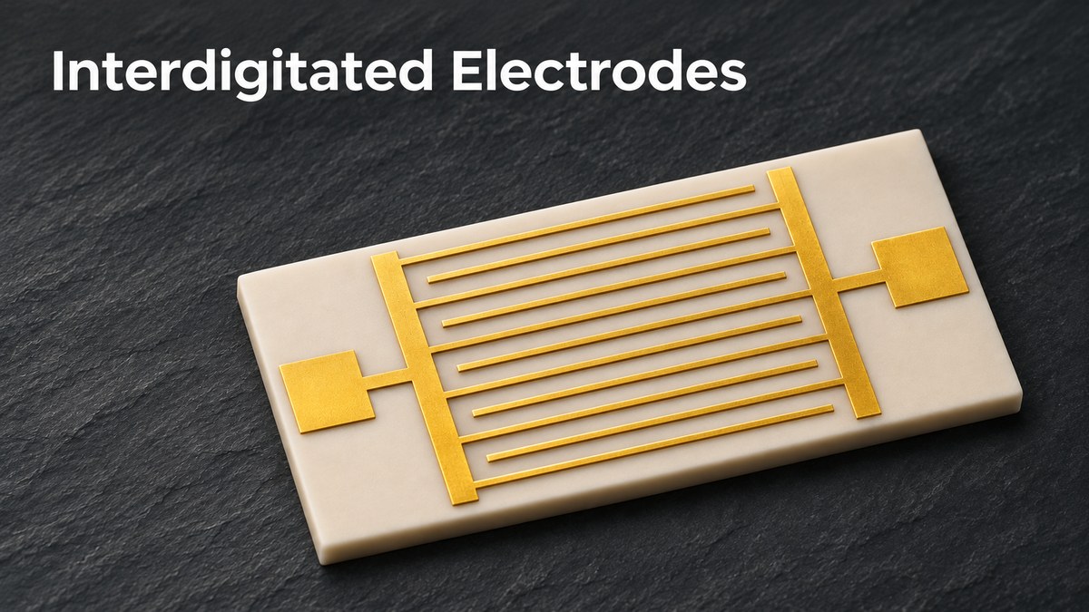
What Are Interdigitated Electrodes and How Do They Work?
Interdigitated electrodes (IDEs) are two electrically separate combs on one surface. The fingers of one comb extend into the gaps of the other. Each comb has its own terminal. What happens between the fingers depends on the test:
- Capacitance. The electric field extends into the substrate and the material above it. A coating or liquid can change the capacitance measured between the terminals.
- Conductance. A conductive film or liquid bridges the gap. Its conductivity and the electrode geometry both influence the reading.
- Impedance. An AC frequency sweep helps distinguish conductive and capacitive contributions. Record the bare-chip response before attributing a change to a sensing film.
When Should You Choose Alumina for an Electrode Prototype?
Alumina suits a top-coated sensor that needs a flat, rigid support. Let the fixture and inspection method narrow the choice.
| Test requirement | Substrate or chip |
|---|---|
| Screen several coatings | Stock alumina IDE |
| Match a fixed seal layout | Custom alumina IDE |
| Inspect through the chip | Glass or quartz |
| Fit a curved surface | Flexible substrate |
- Check the thermal limit of the stack. The electrode, adhesion layer, and connector must also tolerate the coating cure. Alumina’s temperature capability alone cannot qualify the assembled chip.
- Read the selected chip drawing. Schnaiffer’s ready-to-coat alumina series lists gold on a titanium adhesion layer, chip sizes of 10 × 10 or 10 × 25 mm, and nominal finger widths of 100 or 200 µm. Confirm the gap for the selected layout separately. The opaque substrate permits inspection from above.
How Do Finger Width, Gap, and Overlap Affect the Measurement?
Dimension the finished metal. A pitch value alone leaves several possible patterns.
- Width is the distance across one finger. Give the nominal width and allowable variation.
- Gap is the edge-to-edge clearance to the next opposing finger. Changing it changes how the electric field samples the coating and substrate. A smaller gap alone cannot establish a better detection limit.
- Overlap is the length over which opposing fingers run side by side. With other conditions fixed, longer overlap or more finger pairs generally increases capacitance. State the finger count per comb.
For a concrete drawing example, the MicruX ED-IDE2-Pt thin-film device specifies 10 µm width, 5 µm gap, and 120 pairs, with 50 nm of titanium and 150 nm of platinum. Keep that distinction between width and gap when comparing thick-film and thin-film ceramic processes. If the drawing uses pitch, mark both ends of the dimension.
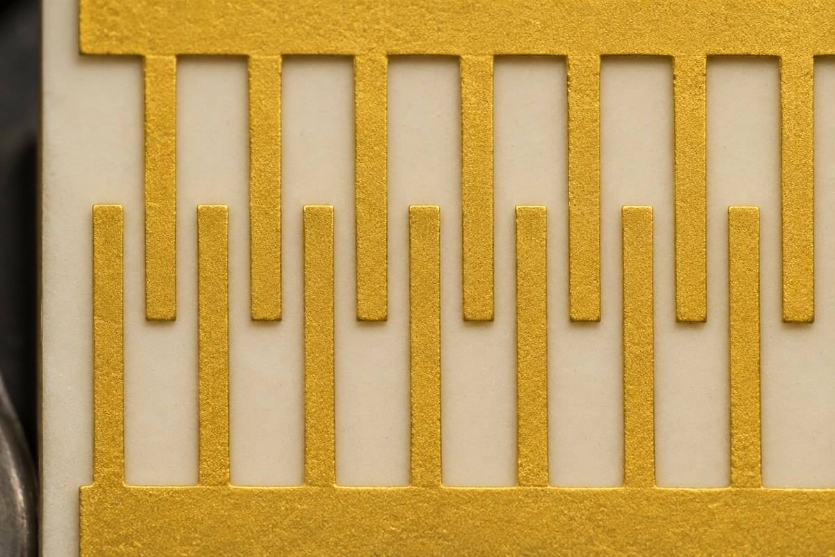
When Should You Specify Gold Electrodes, and Which Areas Need Protection?
Specify exposed gold when the sensing chemistry or measurement protocol requires a gold interface. Confirm compatibility with the sample, cleaning method, and applied potential. Then mark three regions on the drawing:
- Active window. Show which fingers the sample should reach and how far the sensing film should extend.
- Leads. Mark the dielectric cover and its alignment tolerance wherever the liquid must be kept off a lead.
- Pads. Keep enough bare metal outside the coating and seal for the probe or connector to land.
BVT’s CC1.WS conductivity sensor shows why the distinction matters: its platinum-gold alloy electrodes contact the sample, while a dielectric protects the silver leads on the ceramic base.
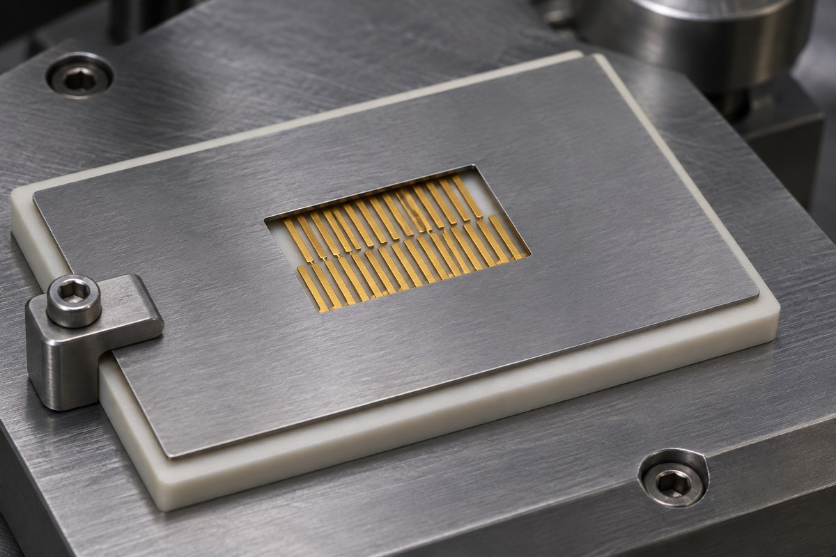
How Do You Test a Bare Electrode Before Applying the Sensing Layer?
Use the bare chip to answer two questions separately: did the pattern meet the drawing, and what does it measure in your fixture?
| Bare-chip check | Acceptance record |
|---|---|
| Pattern dimensions | Width, gap, overlap |
| Finger integrity | Breaks, bridges, pad damage |
| Dry isolation | Test voltage and leakage |
| Impedance baseline | Spectrum and fixture settings |
- Inspect the fingers from above. Measure near both ends and the center of the active window. A continuity reading at a pad can miss a broken finger elsewhere on that comb.
- Separate dry and wet tests. Check isolation on a clean, dry chip at an agreed voltage. Run the reference-medium test separately and record the medium, temperature, excitation amplitude, and frequency range.
- Keep an uncoated control. Compare coated and bare samples with the same fixture, cables, and settings. Otherwise a change in the setup can look like a response from the film.
How Can BSTCeramicPCB Help Review Your Electrode Drawing?
BSTCeramicPCB can review the ceramic pattern for manufacturability and help identify what needs to be verified on a sample. Three inputs make that review more specific:
- Dimensioned layout. Send the outline, active window, finished finger width and gap, tolerances, and pad locations. Include the seal or fixture footprint.
- Material and process. Identify the metal exposed to the sample, the coating solvent, and the cure conditions. For thick-film screen printing on ceramic, BSTCeramicPCB lists 0.10 mm minimum width and 0.10 mm minimum spacing under general capability. The 0.076/0.076 mm special-process entry requires engineering review. A 5 µm gap calls for a separate fabrication assessment.
- Sample acceptance. State the prototype quantity, which dimensions need inspection, and who will apply the sensing film. Agree on bare-chip acceptance before evaluating a coated sensor’s response.
FAQs About Interdigitated Electrodes
Does a 100 µm finger width imply a 100 µm gap?
Only if both dimensions appear on the drawing. Ask for the finished edge-to-edge clearance between adjacent opposing fingers.
Can a bare gold IDE identify a particular gas?
The electrode geometry alone does not establish selectivity. Specify the sensing chemistry, reference conditions, and response test for the target gas.
Can I compare two coatings on chips with different finger counts?
Different geometries can produce different baseline capacitances. Use matched layouts for a coating comparison and record each chip before coating.
Can I inspect the film through the back of an alumina chip?
Alumina is opaque. Plan top-side inspection, or evaluate a transparent substrate if the instrument requires transmitted light.
When is it worth ordering a custom chip?
Use a stock chip if its active area, metal, and pads fit the experiment. A custom layout becomes useful when a gasket crosses the finger array or the holder obscures a contact.
Send your dimensioned layout, coating and test conditions, fixture drawing, and sample quantity to sales@bstceramicpcb.com for a ceramic electrode prototype review.
 Products
 About us
 Contact us