


 HOME
HOME

-

Aluminum Nitride (AlN) Circuit Boards: Revolutionizing Thermal Management in UK Energy Storage Systems
2026 01,10 -
Top Tips for Advanced Semiconductor Packaging Substrate Design
2026 01,05 -
Automotive electronic ceramic circuits make cars smarter and safer
2026 01,05 -
Ceramic PCB for Power Modules (IGBT): The Ultimate High-Thermal Management Guide
2025 12,27 -
Ceramic Substrate or Aluminum PCB for High-Power LEDs
2025 12,24 -
The Ultimate Guide to Alumina Circuit Board (Al2O3): High-Performance Ceramic PCB Solutions for Global Electronics
2025 12,22 -
DBC Welding Strength Compared to Other Materials
2025 12,19 -
LTCC PCB Surprises: What Most People Miss
2025 12,09 -
Comparison of DBC PCBs and MCPCBs for Cooling Performance
2025 12,03 -
Step-by-Step Guide to DPC PCB Design for Sensor Systems
2025 12,03 -
Ceramic PCBs Essential Benefits and Applications
2025 12,01 -
How Al2O3 DPC Ceramic Substrate PCB Enhances Heat Dissipation in Modern Electronics?
2025 11,28 -
How to Choose Between Ceramic, FR4, and Metal Core PCBs
2025 11,27 -
DPC Ceramic PCB Materials: Surprising Science Inside
2025 11,26 -
Wire bondable 2-layer Alumina substrates PCB | Bstceramic PCB
2025 09,22 -
Silicon Nitride Substrate, Silicon Nitride Ceramic Substrate Formula
2025 05,08 -
How to choose the appropriate substrate for ceramic circuit boards?
2023 11,16 -
Laser Cutting or Water Saw Cutting? How To Choose the Best Cutting Solution for Ceramic Circuit Boards
2023 11,13 -
Why Ceramic PCB Is So Expensive?
2023 11,10 -
Which Process Ceramic Circuit Board Is A Better Solution For Semiconductor Refrigerator Chips?
2023 11,06 -
Silicon Printing Circuit Boards For Advancing Electronics
2023 10,27 -
What is the Difference Between HTCC and LTCC Ceramic PCB
2023 10,06 -
What is the Difference Between 96% and 99% Aluminum Oxide in Ceramic PCBs?
2023 09,20 -
Why thick film ceramic PCB is good for oil level sensor in automotive industry?
2023 08,25 -
Silver Paste: The Best Conductor Material for Via Holes in Thick Film Ceramic Boards
2023 08,16 -
Testing Circuit Board Ceramic Diode Fuses: A Complete Guide
2023 08,07 -
Why DBC is replaced by DPC in ceramic PCB manufacturing?
2023 08,01 -
What is thick film ceramic PCB?
2023 08,02
Ceramic Circuit Board Design for the UK Electronics Industry
Table of Contents
- Introduction: Why Ceramic Circuit Board Design Matters
- Understanding Ceramic Circuit Boards
- Key Ceramic Materials Used in the UK Market
- Ceramic Circuit Board Design Principles
- Thermal Management & Reliability Considerations
- Manufacturing Process & DFM for Ceramic PCBs
- Applications Driving Demand in the UK
- Why Choose BST Ceramic PCB
- Conclusion & Next Steps
Ceramic circuit board design has become a critical foundation for high‑reliability electronics in the UK, particularly in sectors such as aerospace, electric vehicles, renewable energy, and industrial automation. Compared with traditional FR‑4 PCBs, ceramic circuit boards offer superior thermal conductivity, electrical insulation, and long‑term stability, making them ideal for harsh operating environments.
For UK engineers and procurement teams, selecting the right ceramic PCB design partner is no longer just about cost—it is about performance, compliance, and lifecycle reliability. This article provides a comprehensive, EEAT‑aligned overview of ceramic circuit board design, integrating best practices from top‑ranking Google results and real manufacturing experience from BST Ceramic PCB.
What Is a Ceramic Circuit Board?
A ceramic circuit board is a type of PCB that uses ceramic materials—rather than epoxy glass—as the substrate. The most common ceramic PCB technologies include:
Thick Film Ceramic PCBs
- Printed conductive pastes on ceramic substrates
- Cost‑effective for medium‑volume production
- Common in power modules and sensors
Thin Film Ceramic PCBs
- High‑precision photolithography
- Excellent line resolution and signal integrity
- Used in RF and microwave applications
DBC (Direct Bonded Copper) Ceramic PCBs
- Copper bonded directly to ceramic
- Outstanding current‑carrying capacity
- Ideal for power electronics and EV systems
Core Ceramic Materials for UK Applications
Material selection is the cornerstone of ceramic circuit board design. UK customers typically prioritize thermal performance, reliability, and RoHS compliance.
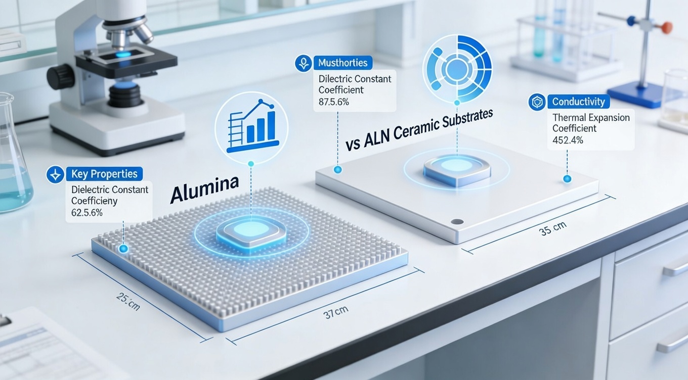
Alumina (Al₂O₃)
- Thermal conductivity: 20–25 W/m·K
- Excellent cost‑performance ratio
- Widely used in industrial and automotive electronics
Aluminum Nitride (AlN)
- Thermal conductivity: up to 170 W/m·K
- Ideal for high‑power and high‑frequency devices
- Popular in aerospace and semiconductor equipment
Silicon Nitride (Si₃N₄)
- High mechanical strength
- Excellent thermal shock resistance
- Emerging choice for next‑generation power modules
Essential Ceramic Circuit Board Design Principles
Designing ceramic circuit boards requires a different mindset compared with standard FR‑4 PCBs.
Layout Optimization
- Minimize thermal resistance paths
- Balance copper distribution to reduce stress
- Avoid sharp corners to prevent crack initiation
Electrical Performance
- Lower dielectric loss for high‑frequency signals
- Stable impedance over temperature
- Suitable for RF and power electronics
Mechanical Reliability
- Match CTE between components and substrate
- Consider solder joint fatigue
- Design for vibration resistance (important for UK rail and aerospace sectors)
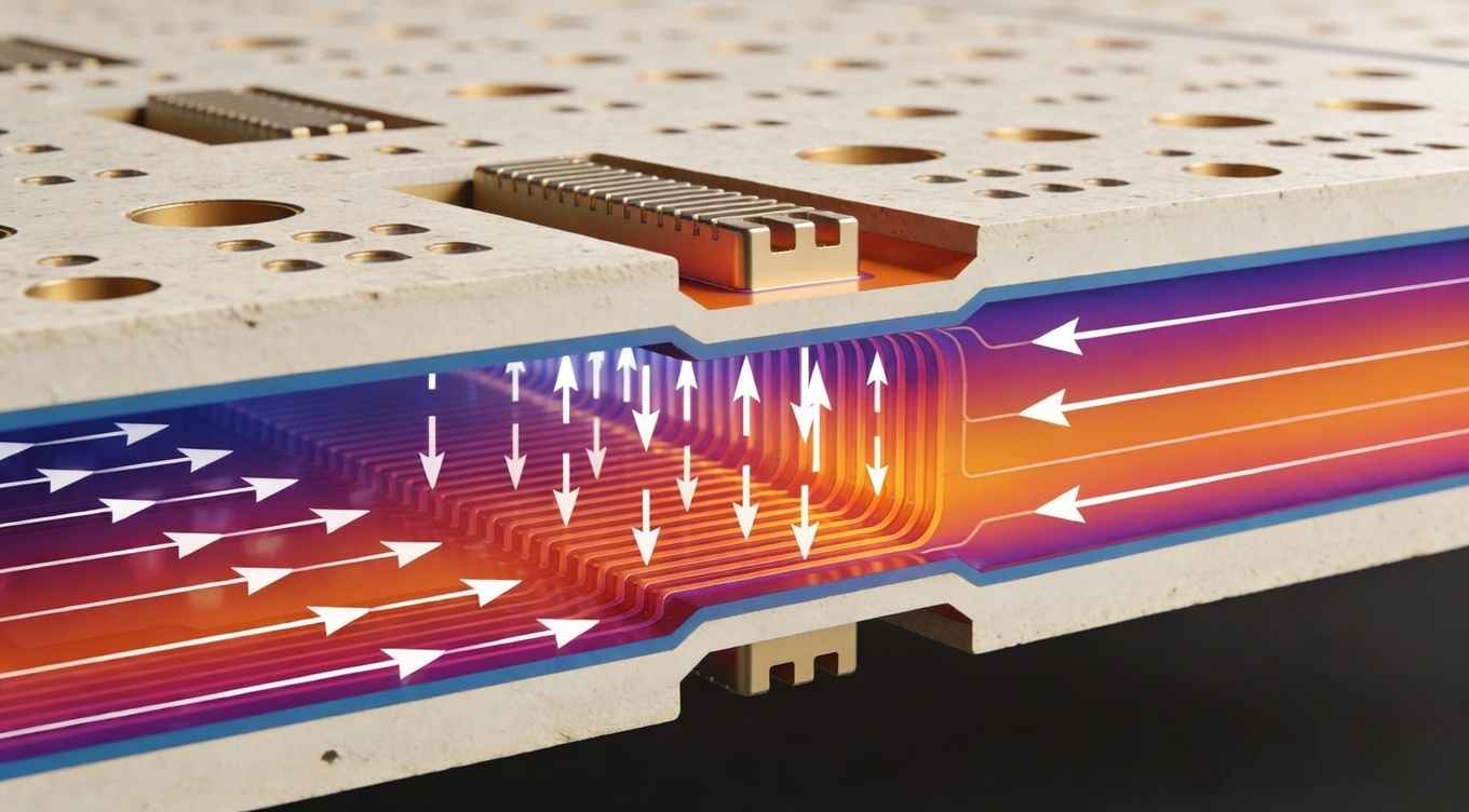
Thermal Management & Long‑Term Reliability
Thermal performance is one of the main reasons UK engineers choose ceramic circuit board design. Ceramic substrates dissipate heat more efficiently, reducing junction temperatures and extending component lifespan.
Heat Dissipation Strategies
- Use DBC structures for power density
- Optimize copper thickness and trace width
- Integrate thermal vias and heat spreaders
Reliability Testing
- Thermal cycling
- High‑temperature storage
- Power cycling for automotive compliance
Manufacturing Process & DFM Considerations
A successful ceramic circuit board design must align with manufacturability. At BST Ceramic PCB, design‑for‑manufacturing (DFM) is integrated from the earliest stage.
Process Overview
- Ceramic substrate preparation
- Copper bonding or metallization
- Circuit patterning
- Surface finishing (ENIG, Ag, Au)
- Electrical and reliability testing
Common DFM Challenges
- Micro‑crack prevention
- Copper‑ceramic adhesion control
- Tight tolerance management
Internal Link Suggestion: Link to Ceramic PCB Manufacturing Process page.
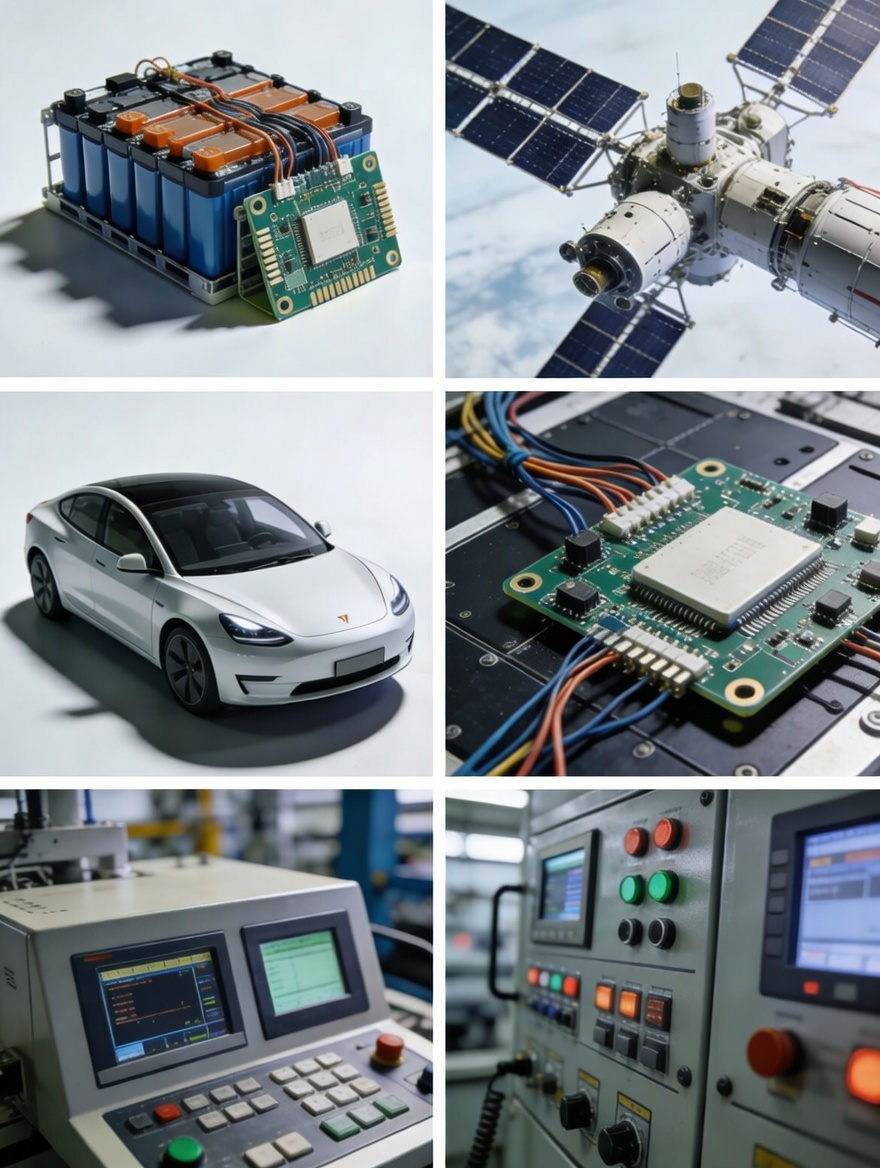
Key Applications Driving UK Demand
Ceramic circuit board design is rapidly expanding across multiple UK industries:
Aerospace & Defence
- Radar systems
- Power control units
- Extreme temperature environments
Electric Vehicles & Charging Infrastructure
- Power modules
- Inverters
- On‑board chargers
Industrial & Renewable Energy
- IGBT modules
- Solar inverters
- Wind power control systems
Why UK Customers Choose BST Ceramic PCB
BST Ceramic PCB combines engineering expertise, advanced manufacturing, and export experience to support UK clients from concept to mass production.
Our Strengths
- In‑house ceramic PCB design support
- ISO‑compliant quality management
- Fast prototyping and scalable production
- Proven export experience to the UK and EU
Engineering Collaboration
Our team works closely with UK engineers to optimize ceramic circuit board design for performance, cost, and reliability.
Internal Link Suggestion: Link to Contact Us or Request a Quote page (high‑conversion form).
Conclusion – Start Your Ceramic Circuit Board Design Project
Ceramic circuit board design is no longer a niche technology—it is a strategic enabler for high‑performance electronics in the UK. By choosing the right materials, following proven design principles, and working with an experienced manufacturer like BST Ceramic PCB, UK companies can achieve higher reliability, better thermal performance, and longer product lifecycles.
 Products
 About us
 Contact us


