


 HOME
HOME

-

Ceramic Circuit Board Design for the UK Electronics Industry
2026 01,13 -
BST Ceramic PCB Expands Small Batch Ceramic PCB Manufacturing Support for Swiss High-Precision Electronics
2026 01,13 -
Aluminum Nitride (AlN) Circuit Boards: Revolutionizing Thermal Management in UK Energy Storage Systems
2026 01,10 -
Top Tips for Advanced Semiconductor Packaging Substrate Design
2026 01,05 -
Automotive electronic ceramic circuits make cars smarter and safer
2026 01,05 -
The Ultimate Guide to Ceramic PCB Air Tightness: Ensuring Hermetic Reliability for High-Performance Electronics in North America
2025 12,29 -
Ceramic PCB for Power Modules (IGBT): The Ultimate High-Thermal Management Guide
2025 12,27 -
Ceramic Substrate or Aluminum PCB for High-Power LEDs
2025 12,24 -
The Ultimate Guide to Alumina Circuit Board (Al2O3): High-Performance Ceramic PCB Solutions for Global Electronics
2025 12,22 -
DBC Welding Strength Compared to Other Materials
2025 12,19 -
LTCC PCB Surprises: What Most People Miss
2025 12,09 -
Comparison of DBC PCBs and MCPCBs for Cooling Performance
2025 12,03 -
Step-by-Step Guide to DPC PCB Design for Sensor Systems
2025 12,03 -
Ceramic PCBs Essential Benefits and Applications
2025 12,01 -
How Al2O3 DPC Ceramic Substrate PCB Enhances Heat Dissipation in Modern Electronics?
2025 11,28 -
How to Choose Between Ceramic, FR4, and Metal Core PCBs
2025 11,27 -
DPC Ceramic PCB Materials: Surprising Science Inside
2025 11,26 -
Wire bondable 2-layer Alumina substrates PCB | Bstceramic PCB
2025 09,22 -
Silicon Nitride Substrate, Silicon Nitride Ceramic Substrate Formula
2025 05,08 -
How to choose the appropriate substrate for ceramic circuit boards?
2023 11,16 -
Laser Cutting or Water Saw Cutting? How To Choose the Best Cutting Solution for Ceramic Circuit Boards
2023 11,13 -
Why Ceramic PCB Is So Expensive?
2023 11,10 -
Which Process Ceramic Circuit Board Is A Better Solution For Semiconductor Refrigerator Chips?
2023 11,06 -
Silicon Printing Circuit Boards For Advancing Electronics
2023 10,27 -
What is the Difference Between HTCC and LTCC Ceramic PCB
2023 10,06 -
What is the Difference Between 96% and 99% Aluminum Oxide in Ceramic PCBs?
2023 09,20 -
Why thick film ceramic PCB is good for oil level sensor in automotive industry?
2023 08,25 -
Statistical analysis of ceramic PCB application fields
2023 08,16 -
Notice of anti-static requirements for PCBA processing and production
2023 08,16 -
Silver Paste: The Best Conductor Material for Via Holes in Thick Film Ceramic Boards
2023 08,16 -
Testing Circuit Board Ceramic Diode Fuses: A Complete Guide
2023 08,07 -
Why DBC is replaced by DPC in ceramic PCB manufacturing?
2023 08,01 -
What is thick film ceramic PCB?
2023 08,02
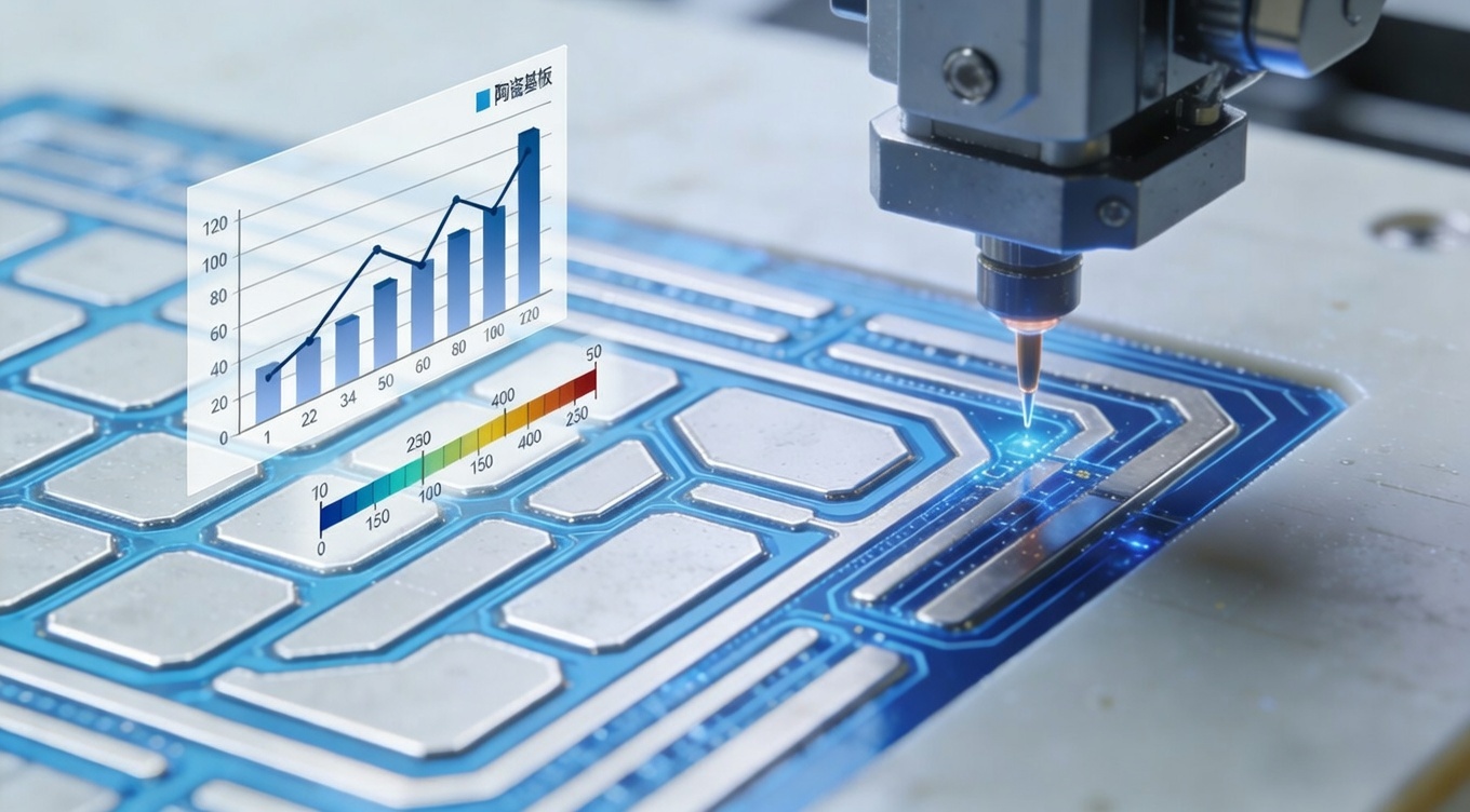
Ceramic Substrate Linewidth and Line Spacing for Power Electronics
Ceramic Substrate Linewidth and Line Spacing: Design Limits and Manufacturing Reality
As power electronics continue to evolve toward higher efficiency, higher power density, and greater reliability, ceramic substrates have become a critical foundation for modern electronic systems. In particular, ceramic substrate linewidth and line spacing play a decisive role in determining electrical performance, thermal stability, and long-term reliability.
For engineers and purchasing teams in Germany—especially in automotive, industrial automation, and renewable energy sectors—understanding the practical limits of ceramic linewidth and spacing is essential. This article provides a realistic, manufacturing-driven perspective on what is achievable today, how design decisions affect production yield, and how to balance performance with cost.
Understanding Linewidth and Line Spacing in Ceramic Substrates
Definition of Linewidth and Line Spacing
Linewidth refers to the width of a conductive trace on a ceramic substrate, while line spacing describes the distance between adjacent traces. Unlike standard FR4 PCBs, ceramic substrates operate under much higher temperatures, voltages, and mechanical stress.
In ceramic PCB manufacturing, linewidth and spacing are influenced not only by design files but also by:
- Metallization method
- Ceramic material properties
- Etching and sintering processes
Why Precision Matters in Power and Automotive Electronics
In high-power applications such as IGBT modules or SiC-based converters, insufficient line spacing can lead to:
-
Electrical breakdown
-
Partial discharge
-
Long-term insulation degradation
German automotive and industrial standards demand consistent electrical clearance, especially for systems operating above 600V or under continuous thermal cycling.
Types of Ceramic Substrates and Their Linewidth Capabilities
Alumina (Al₂O₃) Ceramic Substrates
Alumina remains the most widely used ceramic substrate due to its cost-effectiveness and stable mechanical properties.
Typical achievable values:
- Minimum linewidth: 100–150 μm
- Minimum line spacing: 100–150 μm
Alumina is commonly used in industrial control, LED modules, and medium-power applications.
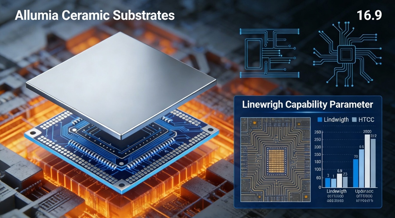
Aluminum Nitride (AlN) Ceramic Substrates
AlN offers superior thermal conductivity, making it ideal for high-power density designs.
Typical achievable values:
- Minimum linewidth: 120–150 μm
- Minimum line spacing: 120–150 μm
Due to its higher material cost and processing complexity, AlN designs often prioritize reliability over extreme miniaturization.
DBC, DPC, and AMB Technology Comparison
| Technology | Typical Linewidth | Typical Spacing | Application Focus |
|---|---|---|---|
| DBC | ≥300 μm | ≥300 μm | High current modules |
| DPC | ≥80–100 μm | ≥80–100 μm | High precision circuits |
| AMB | ≥200 μm | ≥200 μm | Automotive power modules |
Among these, DPC ceramic substrates provide the highest precision, while DBC and AMB prioritize current handling and thermal robustness.
Manufacturing Factors Affecting Ceramic Linewidth and Spacing
Metallization Methods and Etching Precision
Copper thickness, adhesion layers, and etching chemistry directly affect edge definition. In high-precision ceramic PCB manufacturing, maintaining clean trace edges is often more challenging than achieving nominal linewidth.
BST Ceramic PCB applies controlled photolithography and etching processes to ensure consistent trace geometry across production batches.
Substrate Flatness and Thermal Stability
Ceramic substrates undergo high-temperature sintering, which can introduce micro-deformation. Poor flatness may cause:
- Uneven copper thickness
- Localized spacing reduction
- Stress concentration during assembly
Proper material selection and process control are essential to maintain spacing integrity.
Yield Control and Mass Production Consistency
Designs with extremely narrow spacing may work in prototypes but suffer from low yield in volume production. For German OEMs, stable mass production often outweighs marginal gains in miniaturization.
Design Guidelines for Optimizing Linewidth and Line Spacing
Electrical Performance Considerations
When defining ceramic linewidth:
- Wider traces reduce resistive losses
- Adequate spacing prevents arcing and EMI issues
Designers should align trace geometry with actual operating voltage, not theoretical limits.
Thermal and Mechanical Reliability
Narrow traces experience higher thermal stress under current load. For power modules, slightly increasing linewidth often improves lifetime performance without significantly increasing substrate size.
Compliance with IPC and Automotive Standards
Common references include:
- IPC-2221 (Generic PCB Design)
- IPC-6012DA (High Reliability Applications)
- Automotive OEM internal standards
BST Ceramic PCB supports design reviews aligned with European and automotive compliance requirements.
Typical Applications in the German Market
Automotive Power Modules
Ceramic substrates are widely used in:
- Inverters
- On-board chargers
- DC-DC converters
Line spacing is especially critical for high-voltage isolation and long-term reliability.
Industrial Power Electronics
Applications include:
- Motor drives
- Power supplies
- Industrial automation systems
Here, robust spacing often takes priority over ultra-fine linewidth.
Renewable Energy and EV Charging Systems
Solar inverters and EV chargers require ceramic substrates capable of withstanding high voltage and outdoor thermal cycling, making conservative spacing a preferred design choice.
Why Choose BST Ceramic PCB for High-Precision Ceramic Substrates
Manufacturing Capability Overview
BST Ceramic PCB specializes in:
- Alumina and AlN ceramic substrates
- DPC, DBC, and AMB technologies
- Precision linewidth and spacing control
Our engineering team supports design-for-manufacturing (DFM) analysis to balance performance and yield.
Quality Control and Engineering Support
From prototype to mass production, BST implements:
- Process traceability
- Electrical and visual inspection
- Reliability-focused design feedback
Conclusion: Balancing Design Ambition and Manufacturing Reality
Achieving optimal ceramic substrate linewidth and line spacing is not about pushing theoretical limits, but about aligning design intent with manufacturing reality. For German manufacturers focused on reliability, safety, and long product lifecycles, a well-balanced approach delivers the best results.
By combining engineering expertise with controlled manufacturing processes, BST Ceramic PCB helps customers translate design concepts into reliable, scalable ceramic substrate solutions.
 Products
 About us
 Contact us


