


 HOME
HOME

-

High-Temperature Resistant Ceramic PCB Solutions for Industrial LTCC and HTCC Applications
2026 01,15 -
Ceramic Circuit Board Design for the UK Electronics Industry
2026 01,13 -
Aluminum Nitride (AlN) Circuit Boards: Revolutionizing Thermal Management in UK Energy Storage Systems
2026 01,10 -
Top Tips for Advanced Semiconductor Packaging Substrate Design
2026 01,05 -
Automotive electronic ceramic circuits make cars smarter and safer
2026 01,05 -
Ceramic PCB for Power Modules (IGBT): The Ultimate High-Thermal Management Guide
2025 12,27 -
Ceramic Substrate or Aluminum PCB for High-Power LEDs
2025 12,24 -
The Ultimate Guide to Alumina Circuit Board (Al2O3): High-Performance Ceramic PCB Solutions for Global Electronics
2025 12,22 -
DBC Welding Strength Compared to Other Materials
2025 12,19 -
LTCC PCB Surprises: What Most People Miss
2025 12,09 -
Comparison of DBC PCBs and MCPCBs for Cooling Performance
2025 12,03 -
Step-by-Step Guide to DPC PCB Design for Sensor Systems
2025 12,03 -
Ceramic PCBs Essential Benefits and Applications
2025 12,01 -
How Al2O3 DPC Ceramic Substrate PCB Enhances Heat Dissipation in Modern Electronics?
2025 11,28 -
How to Choose Between Ceramic, FR4, and Metal Core PCBs
2025 11,27 -
DPC Ceramic PCB Materials: Surprising Science Inside
2025 11,26 -
Wire bondable 2-layer Alumina substrates PCB | Bstceramic PCB
2025 09,22 -
Silicon Nitride Substrate, Silicon Nitride Ceramic Substrate Formula
2025 05,08 -
How to choose the appropriate substrate for ceramic circuit boards?
2023 11,16 -
Laser Cutting or Water Saw Cutting? How To Choose the Best Cutting Solution for Ceramic Circuit Boards
2023 11,13 -
Why Ceramic PCB Is So Expensive?
2023 11,10 -
Which Process Ceramic Circuit Board Is A Better Solution For Semiconductor Refrigerator Chips?
2023 11,06 -
Silicon Printing Circuit Boards For Advancing Electronics
2023 10,27 -
What is the Difference Between HTCC and LTCC Ceramic PCB
2023 10,06 -
What is the Difference Between 96% and 99% Aluminum Oxide in Ceramic PCBs?
2023 09,20 -
Why thick film ceramic PCB is good for oil level sensor in automotive industry?
2023 08,25 -
Silver Paste: The Best Conductor Material for Via Holes in Thick Film Ceramic Boards
2023 08,16 -
Testing Circuit Board Ceramic Diode Fuses: A Complete Guide
2023 08,07 -
Why DBC is replaced by DPC in ceramic PCB manufacturing?
2023 08,01 -
What is thick film ceramic PCB?
2023 08,02
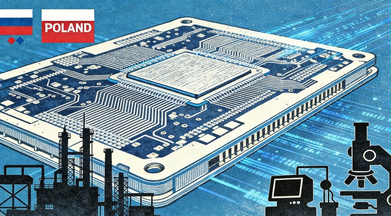
Ceramic Substrate Custom Solutions for Poland’s High-Tech Sectors: Engineering Precision & Thermal Efficiency
Table of Contents (Quick Navigation)
- The Rising Demand for Ceramic PCBs in Poland's Electronics Industry
- Material Selection: Alumina (Al2O3) vs. Aluminum Nitride (AlN) for Custom Projects
- Deep Dive: DPC vs. DBC Technologies in Customization
- Key Design Parameters for Custom Ceramic Substrates
- Why Polish Engineers Choose BESTFPC as Their Strategic Partner
The Rising Demand for Ceramic PCBs in Poland's Electronics Industry
Poland has firmly established itself as the heart of Europe’s electronics manufacturing services (EMS) sector. From the industrial clusters in Lower Silesia to the tech hubs in Warsaw, the demand for high-performance interconnect solutions is skyrocketing. Unlike traditional FR-4 PCBs, which struggle under the thermal loads of modern power electronics, Ceramic Substrate Custom solutions are becoming the mandatory standard for engineers aiming to compete in the EU market.
The shift is driven by three specific sectors where BST Ceramic PCB (BESTFPC) has observed a 40% year-over-year increase in inquiries from Polish clients:
- E-Mobility & Automotive: Poland is a leading player in the European EV battery supply chain. The Battery Management Systems (BMS) and On-Board Chargers (OBC) require substrates that can handle massive currents while maintaining structural integrity. Our ceramic solutions offer a Coefficient of Thermal Expansion (CTE) closely matched to Silicon (Si) chips, ensuring reliability even under the extreme thermal cycling of Polish winters and operational heat.
- High-Power LED Lighting: Industrial and automotive lighting manufacturers in Poland face the challenge of "lumen droop" caused by heat. Custom ceramic substrates provide a direct thermal path, eliminating the need for bulky heatsinks and allowing for sleeker, more efficient designs.
- Industrial Power Modules: In heavy machinery and renewable energy inverters (photovoltaic), voltage breakdown is a critical failure mode. BST’s custom substrates offer high dielectric strength, ensuring safety and longevity in high-voltage applications.
For Polish procurement managers and R&D engineers, the question is no longer if they need ceramic substrates, but how to customize them for optimal cost-performance ratio. This is where BESTFPC’s expertise bridges the gap between concept and mass production.
Material Selection: Alumina (Al2O3) vs. Aluminum Nitride (AlN) for Custom Projects
When configuring a Ceramic Substrate Custom order, the first decision determines 80% of the board's thermal performance: the base material. At BST, we guide our Polish clients through a rigorous selection process based on thermal conductivity ($k$) and budget constraints.
1. Alumina (Al2O3) – The Cost-Effective Workhorse
For 96% of standard applications, 96% Alumina is the industry standard. It offers a thermal conductivity of approximately $20-24 W/m\cdot K$. While this is significantly higher than FR-4 (which is typically $<1.0 W/m\cdot K$), it is an entry-level ceramic option.
- Best for: General LED lighting, sensor modules, and consumer electronics where cost sensitivity is high but standard PCBs fail.
- BST Customization: We offer thickness customization from 0.25mm to 1.0mm, with options for 99.6% purity for high-frequency applications requiring lower dielectric loss.
2. Aluminum Nitride (AlN) – The Premium Heat Spreader
For the high-end Polish power electronics market, AlN is the superior choice. With a thermal conductivity ranging from $170 W/m\cdot K$ to $230 W/m\cdot K$, AlN dissipates heat nearly 8 times faster than Alumina.
- Best for: IGBT modules, high-power laser diodes, and EV power inverters where heat density is critical.
- The Polish Context: As Poland integrates deeper into the EU's green energy grid, the efficiency gains from AlN substrates in power converters justify the higher material cost.
- Technical Note: AlN’s CTE ($~4.6 ppm/°C$) is a near-perfect match for Silicon ($~4.2 ppm/°C$) and Gallium Nitride (GaN). This minimizes mechanical stress on solder joints during operation, a critical factor for reliability certifications.
Decision Matrix for Buyers:
If your device power density exceeds $100 W/cm^2$, BST strongly recommends moving directly to Aluminum Nitride custom substrates to prevent early component failure.
Deep Dive: DPC vs. DBC Technologies in Customization
A truly Ceramic Substrate Custom project requires selecting the right metallization technology. This is often where "off-the-shelf" suppliers fail to meet the specific engineering requirements of sophisticated Polish designs. BST specializes in three core technologies, but two are dominant:
1. Direct Bonded Copper (DBC)
DBC involves bonding copper foil to the ceramic using a high-temperature eutectic bond (over $1000°C$).
- Pros: Extremely thick copper layers (up to $300-500\mu m$) allow for massive current carrying capacity. Ideal for power electronics.
- Cons: Limited resolution. You cannot achieve fine lines or tight spacing (trace/space usually limits at $150-200\mu m$).
- Customization: BST can customize the copper thickness to balance current load vs. cost.
2. Direct Plated Copper (DPC)
This is where BST excels for precision applications. DPC utilizes vacuum sputtering (PVD) followed by electroplating.
- The BST Advantage: We can achieve incredible precision.
- Trace Width/Space: Down to $50\mu m$ (or even lower for specific custom batches).
- Through-Holes: DPC allows for reliable manufacturing of copper-filled vias (interconnects), enabling 3D stacking and double-sided circuitry on ceramics, which is difficult with DBC.
- Surface Flatness: DPC offers superior flatness, crucial for wire bonding and flip-chip assembly widely used in Poland’s microelectronics assembly lines.
Hybrid Solutions:
For complex inquiries from Poland, we sometimes suggest AMB (Active Metal Brazing) for extreme reliability, particularly in aerospace or military-grade specs. Understanding the trade-off between DPC's precision and DBC's power is vital.
Key Design Parameters for Custom Ceramic Substrates
To ensure your inquiry results in a "Manufacturable" design rather than a rejection, understanding the customization limits is key. At BST Ceramic PCB, we process hundreds of Gerber files monthly. Here is a checklist for Polish engineers optimizing their designs for our production lines:
1. Board Thickness & Dimensions:
Standard ceramic master plates often come in $114 \times 114mm$ or $127 \times 127mm$. Customizing your single board size to maximize utilization of this master plate can save up to 30% in material waste.
- Standard Thickness: 0.38mm, 0.50mm, 0.635mm (most common), 1.0mm.
- Custom Tip: Avoid requesting non-standard thicknesses (e.g., 0.55mm) unless volume warrants a custom mold run, as this increases lead time.
2. Surface Finish (The Interface):
For the Polish market, where RoHS compliance is non-negotiable, we offer:
- ENIG (Electroless Nickel Immersion Gold): The gold standard for flat surfaces and reliable soldering.
- ENEPIG: Excellent for gold wire bonding reliability.
- Immersion Silver: A cost-effective alternative for lighting applications.
3. Metal Layer Structure:
In a Ceramic Substrate Custom order, you must specify the Copper-Nickel-Gold stack up. For example, a typical DPC spec might be: $10\mu m - 50\mu m$ Copper + $3\mu m - 5\mu m$ Nickel + $0.05\mu m$ Gold.
- Warning: Too much copper on a thin ceramic base without balancing stresses can lead to bowing or cracking. Our engineering team performs Design for Manufacturing (DFM) checks on every file to prevent this.
4. Solder Mask & Silkscreen:
- Unlike FR-4, the adhesion of solder mask on ceramic surfaces requires specific polymer formulations. We use high-temperature resistant white or black glazes that maintain color stability even after multiple reflow cycles—vital for LED applications where color reflection matters.
Why Polish Engineers Choose BSTCERAMICPCB as Their Strategic Partner
The Polish market is flooded with traders, but finding a direct manufacturer with Ceramic Substrate Custom expertise is rare. Here is why BST (BESTFPC) is capturing the market share in Central Europe:
1. "Factory Direct" Transparency
We are not a middleman. When you submit an inquiry form on bstceramicpcb.com, you are speaking directly to the factory floor. This means:
- Competitive Pricing: No broker markups.
- Technical Clarity: Direct access to CAM engineers who understand Polish/EU technical standards.
2. Rapid Prototyping for R&D
We understand that Polish design houses work on tight innovation cycles.
- Lead Time: We offer expedited prototype services (Quick Turn) for ceramic boards, often delivering samples in as little as 5-7 working days, allowing you to validate your design faster than your competitors.
3. Rigorous Quality Control (The EEAT Factor)
We don't just ship boards; we ship data. Every batch of custom ceramic substrates undergoes:
- High Voltage Testing: Ensuring dielectric breakdown thresholds are met.
- Thermal Conductivity Verification: Using laser flash analysis methods.
- AOI (Automated Optical Inspection): To catch micron-level trace defects.
- Vacuum Packaging: To prevent oxidation during shipping to Poland.
4. Optimized Logistics to Poland
We have established logistics routes to major Polish hubs (Warsaw, Lodz, Wroclaw). We handle the documentation to ensure smooth customs clearance, understanding the VAT and import regulations pertinent to EU trade.
Conclusion & Next Steps
Your high-performance electronics deserve a foundation that won't fail. Whether you are designing the next generation of EV chargers in Silesia or LED arrays in Warsaw, BST is your partner for Ceramic Substrate Custom excellence.
 Products
 About us
 Contact us


