-

Silicon Nitride Substrate, Silicon Nitride Ceramic Substrate Formula
2025 05,08 -

How to choose the appropriate substrate for ceramic circuit boards?
2023 11,16 -

Laser Cutting or Water Saw Cutting? How To Choose the Best Cutting Solution for Ceramic Circuit Boards
2023 11,13 -

Why Ceramic PCB Is So Expensive?
2023 11,10 -

Which Process Ceramic Circuit Board Is A Better Solution For Semiconductor Refrigerator Chips?
2023 11,06 -

Silicon Printing Circuit Boards For Advancing Electronics
2023 10,27 -

What is the Difference Between HTCC and LTCC Ceramic PCB
2023 10,06 -

What is the Difference Between 96% and 99% Aluminum Oxide in Ceramic PCBs?
2023 09,20 -

Why thick film ceramic PCB is good for oil level sensor in automotive industry?
2023 08,25 -

Statistical analysis of ceramic PCB application fields
2023 08,16 -

Notice of anti-static requirements for PCBA processing and production
2023 08,16 -

Silver Paste: The Best Conductor Material for Via Holes in Thick Film Ceramic Boards
2023 08,16 -

Testing Circuit Board Ceramic Diode Fuses: A Complete Guide
2023 08,07 -

Why DBC is replaced by DPC in ceramic PCB manufacturing?
2023 08,01 -

What is thick film ceramic PCB?
2023 08,02
- Ceramic PCB
- Alumina PCB
- Alumina Ceramic PCB
- HTCC ceramic PCB
- Thin Film Ceramic PCB
- Ceramic PCB Design
- ceramic substrate
- HTCC Ceramic Substrate Selection
- AlN Ceramic PCB
- AlN PCB
- Quality Control
- DPC Ceramic Substrate
- Surface Treatment
- alumina ceramic substrate
- Ceramic PCB Performance
- What HTCC Ceramic PCB
- Thermal conductivity
- Thick Film Ceramic PCB Application
- glass glaze
- Direct Bonded Copper
- Ceramic Materials
- ceramic pcb assembly
- ceramic pcb material
- Aluminum Nitride Ceramic PCB
- What is thin film ceramic PCB
- Active Metal Brazing
- Ceramic Metallization Technology
- Laser Cutting
- Via Hole
- X-ray
- ceramic pcb manufacturer
- DBC Ceramic PCB
- AMB Ceramic Substrate
- ceramic circuit board
- LTCC Ceramic PCB
- 3D AOI
- What DCB PCB
- Conductive Silver Paste
- Oil Level Sensor PCB
- Blister Box Packing
- Manufacturing Process
- What AMB Ceramic PCB
- AMB PCBA
- DBC PCB Instead
- Conductive Pastes
- DCB Manufacturing Process
- Components Mount
- Water Absorption
- Company Profile
- alumina material
- Substrate Drilling And Outline Cutting
- Applications of Ceramic PCB
- DBC Ceramic PCB Application
- Types Of Thick Film Ceramic PCB
- alumina cte
- Directly Bonded Copper
- Direct Plating Copper PCB Assembly
- Maximum Size Of Thick Film Ceramic PCB
- What LTCC Ceramic PCB
- alumina ceramic material
- Samp Making
- Ceramic PCB superior thermal conductivity
- Rigorous Testing And Inspection
- Applications Of Ceramic Circuit Board
- Solder Mask
- ceramic pcb vs fr4 pcb
- Via Filling
- DPC vs DBC
- Ceramic PCB Resistors
- Advantages Of LTCC Ceramic PCB
- Thick Film Substrate Raw Materials
- 100% Raw Material Guarantee
- ISO 13485:2016
- Plug-in Component
- al2o3 substrate price
- HTCC Ceramic Substrate Selecti
- silicon nitride vs silicon carbide
- Debris Management And Contamination Prevention
- Staff Operating Norms
- protect your information
- aluminum nitride ceramic substrate
- Reduction Atmosphere Sintering
- Ceramic PCB vs Other PCBs
- In-process Quality Control
- Scoreboard
- Engineering Specifications
- electric permittivity of ceramic substrate
- DPC Ceramic PCB Fabrication
- Suitable PCB For Aerospace
- Sintering Performance
- Peak Sintering Temperature
- Drilling
- What DPC Ceramic PCB
- Silicone Circuit Board
- DBC Manufacturing Capability
- Oxidation Treatment
- Thin Film Technology
- aluminum nitride thermal conductivity
- How To Produce Thick Film Ceramic PCB
- ceramic PCB manufacturers
- Budget Constraints
- Silver Paste Via
- Etching Process
- DCB PCB Printing Process
- Surface Electrode Silver Paste
- Oil Level Sensor Ceramic PCB Advantages
- Thick Film Ceramic Board Via Hole
- Application
- what is aluminum nitride
- Features of Active Metal Braze Ceramic PCB
- Ceramic PCB Type
- HTCC PCB Assembly
- Testing Ceramic PCB Diodes
- AgPd Paste Thickness
- alumina board
- DBC PCB Making Process
- Ceramic PCB vs Aluminum Core PCB
- Visual Inspection
- Package Types For Ceramic Circuit Board
- depanelize ceramic pcb
- AMB Ceramic PCB Manufacturing Processes
- Thick Film PCBA
- HTCC Ceramic PCB Application
- Aluminum Nitride
- al2o3 aluminum substrate
- Depanelization
- alumina cte vs temperature
- Solder Paste Selection
- Insulation Materials
- Best Technology
- Printing Resistance Ink
- ceramic PCB stability
- SGS
- Thin Film Ceramic PCB Application
- Standar Thickness
- Collatingstacking Process
- alumina ceramic
- Line Width Of Thick Film Ceramic Board
- is alumina ceramic durable
- Blackening Spot Removing
- QA System
- UL
- Advantages Of Plug-in Components
- How To Fabricate HTCC Ceramic PCB
- silicon nitride substrate
- HTCC vs LTCC
- Ceramic PCB Market
- Peak Temperature Soak Time
- Whats HTCC Ceramic PCB
- Conductor Material for HTCC Ceramic PCB
- Pre-production Inspection
- Drilling Hole
- SMD
- Production Processes Of LTCC Ceramic PCB
- silicon nitride ceramic substrate
- Red Coating
- Factory Safe Production
- De-panel Separate
- Silicon Nitride Dielectric Constant
- How to production DPC PCB
- Cooling Instrument Circuit Board
- LTCC Manufacturing Capability
- Conductor Substrate
- What is thick film ceramic PCB
- direct bonded copper substrate
- Thick Film Ceramic Substrate Fabrication
- AIN ceramic PCB
- Aerospace Ceramic PCB
- High Conductivity
- What Kinds Of Alumina Substrate
- End-contact Electrode Silver Paste
- DPC Manufacturing Capability
- Thin Film Manufacturing Process
- aluminum nitride coating
- AMB PCB Application
- 96% Aluminum Oxide
- Testing Ceramic Diode Fuses
- Operating Temperature
- heavy copper pcb
- Copper Foil Preparation
- DBC Ceramic PCB Structure
- Vacuum Packaging
- Thin Film Structure And Composition
- AMB Ceramic Substrates PCB Fabrication Processes
- Ceramic PCB excellent thermal
- DBC PCBA
- Advantages Of DPC PCB
- Different Colors Of Thick Film Ceramic PCB
- DCB Fabrication
- First Article Inspection
- How To Connect Paste And Materials
- Corporate Values
- Thick Film Substrate Raw Materials
- Advantages of ordinary PCB
- ANSI
- DPC Ceramic PCB Application
- E-test
- Directly Copper Plating
- DPC PCB Assembly
- Thick Film Ceramic Substrate Bonded
- Disadvantage Of LTCC PCB
- Conductive Ink Preparation
- Coefficient Of Expansion
- LQAS
- Ceramic PCB Certification
- Plug-in Component Tips
- ceramic pcb cost
- Via Punching And Cavity Process
- 900℃ PCB vs 1500℃ PCB
- Ceramic PCB Sintering Cycle
- Disadvantages Of LTCC Ceramic PCB
- Conductor Material for HTCC Ceramic PCB
- Ceramic PCB Fabrication
- PPI
- ISO 9001:2015
- SMD Technology
- al2o3 substrate
- How To Fabricate LTCC Ceramic PCB
- silicon nitride melting point
- Reduced Risk Of Broken
- Work Notice
- privacy policy
- LTCC Ceramic Substrates
- Air Sintering
- Why Ceramic PCB So Expensive
- Jigsaw Puzzle
- The Future of Thick Film Ceramic PCB
- ceramic material
- How To Produce DPC Ceramic PCB
- Aerospace PCB Material
- Chemical Stability And Reliability
- Conduct Material Dielectric Constants
- ceramic circuit boards
- What DBC Ceramic PCB
- Silicone Ceramic PCB
- Thin Film PCB Manufacturing Capability
- Conductive Paste
- aluminum nitride material properties
- Thick Film Ceramic PCB Manufacturing Processes
- Thick film PCB
- Project Requirements
- Silver Paste
- Printing Process
- Etching
- AMB PCB Yielding Process
- Internal Electrode Silver Paste
- Why Choose Thick Film Ceramic PCB For Ceramic PCB
- Thin Film Vs Thick Film
- aluminum pcb
- Manufacturing Process Of AMB Ceramic PCB
- LTCC PCB Assembly
- Why DPC PCB Instead Of DBC PCB
- Conductive Paste Thickness
- ceramic substrate manufacturer
- How To Produce DCB Ceramic PCB
- Active Metal Brazed
- Reflow Soldering
- Waterproof Ability
- BST Ceramic PCB
- how to de-panel ceramic pcb
- Ceramic PCB advantages
- Thin Film PCBA
- LTCC Ceramic PCB Application
- Aluminum Oxide
- 96% alumina
- DBC PCB Manufacturing Process
- Stencil Preparation
- Ceramic PCB Insulation
- LTCC Ceramic PCB Manufacturing Processes
- how to make alumina
- Spreading Drying
- Ceramic circuit board application
- Conductor Printing
- how to cut alumina ceramic
- Difference Between DPC And DBC
- Ceramic PCB Resistance
- What
- cutting alumina
- Substrate Drilling And Outline Cutting
- Electronic Packing Material
- IATF 16949:2016
- Types Of Plug-in Components
- ceramic circuit board price
- HTCC Ceramic PCB Fabrication Processes
- silicon nitride formula
- Improved Yield And Efficiency
- Ceramic PCB Application Analysis
- personal information
- Value Of Ceramic PCBs
- Quality Control In Production
- Ceramic Substrate Hole
- Thick Film PCB Application
- DPC Ceramic PCB Manufacturing
- Red Ink
- Adhesion And Rheology
- Peak Sintering Temperature Of Thick Film Ceramic PCB
- Solder Mask Surface Finishing
- ceramic pcb board
- DPC Manufacturing Process
- Semiconductor Refrigerator PCB
- AMB Manufacturing Capability
- AgPd Oxidize
- Thin Film PCB Definition
- 2nd Laminate And Etching
- Device Design
- Advantages Of Silver Paste
- Kinds Of Alumina Substrate
- DCB PCB Structure
- Via-fill Electrode Silver Paste
- Gold Paste
- Thin Film Application
- aluminum nitride formula
- Active Metal Braze Ceramic PCB
- BSTCeramicPCB
- Ceramic PCB Diode Fuses
- Au Paste Thickness
- Ceramic Substrate Preparation
- How to choose between MCPCB and Ceramic PCB
- How To Pack General Ceramic Circuit Boards
- Key Features And Advantages
- How to produce AMB Ceramic PCB
- Ceramic PCB with different resistances
- DPC PCBA
- DBC vs DPC
- Beryllium Oxide
- aluminum substrate
- FQC
- direct bonded copper ceramic PCB
- Solder Paste Printing
- Connection Between Conductive Paste And Materials
- Company Culture
- alumina substrate
- Printing Glass Glaze
- IPC
- AMB Ceramic PCB Application
- Screen Printed
- amb ceramic pcb
- Sinteringco-firing
- Molybdenum Manganese
- Line Spacing Of Thick Film Ceramic Board
- Advantage Of LTCC PCB
- Make Stencil
- Dielectric Constant
- IPQC
- SGS Institution
- How to assemble plug-in component
- ceramic pcb price
- Green Tap
- alumina circuit board
- High Temperature Co-fired vs Low Temperature Co-fired
- Five Major Application Areas
- Sintering Cycle
- HTCC PCB Manufacturing Processes
- how to cut alumina
- HTCC Ceramic Substrate Selection
- Water Saw Cutting
- Laser Drilling Hole
- SMD VS SMT
- ceramic metallization
- LTCC PCB Manufacturing Processes
- silicon nitride material
- DPC PCB Pretection Process
- Ceramic PCBA Static Protection
- HTCC Ceramic Substrate Selection
- Si3N4 Material Properties
- Ceramic PCB For Cooling
- HTCC Manufacturing Capability
- Characteristics of Thick Film Ceramic PCB
- ceramic heat resistance
- Making Process Of DPC Ceramic PCB
- DPC ceramic substrates
- Aerospace Application PCB Choice
- Compatibility With Ceramic Substrates
- Dielectric Constants
- ceramic circuit board material
- Conductor Material for HTCC Ceramic PCB
- Silicone PCB
- Thick Film PCB Manufacturing Capability
- Special Silver Paste
- How To Manufacture Thin Film Ceramic PCB
- aluminum nitride sheet
- Capability Of AMB Ceramic PCB
- 99% Aluminum Oxide
- Circuit Diodes
- Can thick film ceramic board use copper as conductor?
- Bonding
-
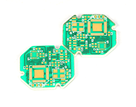
HTCC Ceramic PCB Fabrication Processes
Actually, the manufacturing for HTCC Ceramic Substrate PCB is the same as LTCC PCB, only the co-fired temperature is above 1500 Celsius while LTCC should be sintered under 1000 Celsius. Fabrication processes for HTCC Ceramic PCB: 1. Green tap; 2. Via punching and cavity process; 3. Via filling; 4. Conductor printing; 5. Collating/stacking process; 6. Sintering/co-firing; 7. E-test; 8. Surface treatment; 9. Laser cutting; 10. Depanelization; 11. FQC. 2023-05-08 -
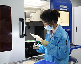
Laser Cutting or Water Saw Cutting? How To Choose the Best Cutting Solution for Ceramic Circuit Boards
Laser cutting and water saw cutting have their own advantages and disadvantages in ceramic circuit board manufacturing, BSTCeramicPCB welcomes to know more. 2023-11-13






























 HOME
HOME


