


 HOME
HOME

-

Automotive-grade Aluminum Nitride Substrate in Europe — Technical Specifications, Applications, and Supplier Selection
2026 01,23 -
Ceramic PCB Solutions in Sweden: Technical Requirements, Industry Applications, and Supplier Selection Strategy
2026 01,21 -
Ceramic Substrate Custom Solutions for Poland’s High-Tech Sectors: Engineering Precision & Thermal Efficiency
2026 01,20 -
High-Temperature Resistant Ceramic PCB Solutions for Industrial LTCC and HTCC Applications
2026 01,15 -
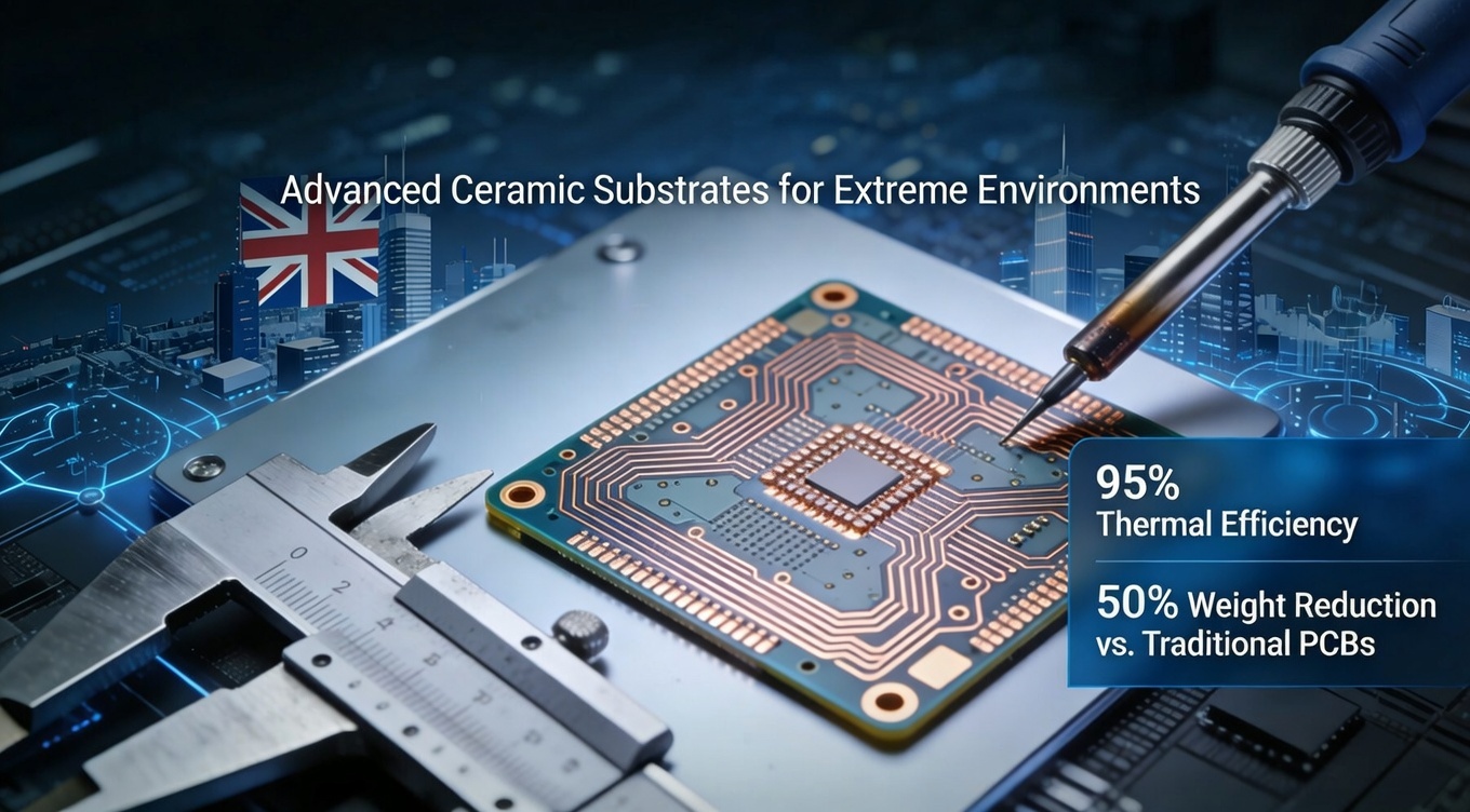
Ceramic Circuit Board Design for the UK Electronics Industry
2026 01,13 -
Aluminum Nitride (AlN) Circuit Boards: Revolutionizing Thermal Management in UK Energy Storage Systems
2026 01,10 -
Top Tips for Advanced Semiconductor Packaging Substrate Design
2026 01,05 -
Automotive electronic ceramic circuits make cars smarter and safer
2026 01,05 -
Ceramic PCB for Power Modules (IGBT): The Ultimate High-Thermal Management Guide
2025 12,27 -
Ceramic Substrate or Aluminum PCB for High-Power LEDs
2025 12,24 -
The Ultimate Guide to Alumina Circuit Board (Al2O3): High-Performance Ceramic PCB Solutions for Global Electronics
2025 12,22 -
DBC Welding Strength Compared to Other Materials
2025 12,19 -
LTCC PCB Surprises: What Most People Miss
2025 12,09 -
Comparison of DBC PCBs and MCPCBs for Cooling Performance
2025 12,03 -
Step-by-Step Guide to DPC PCB Design for Sensor Systems
2025 12,03 -
Ceramic PCBs Essential Benefits and Applications
2025 12,01 -
How Al2O3 DPC Ceramic Substrate PCB Enhances Heat Dissipation in Modern Electronics?
2025 11,28 -
How to Choose Between Ceramic, FR4, and Metal Core PCBs
2025 11,27 -
DPC Ceramic PCB Materials: Surprising Science Inside
2025 11,26 -
Wire bondable 2-layer Alumina substrates PCB | Bstceramic PCB
2025 09,22 -
Silicon Nitride Substrate, Silicon Nitride Ceramic Substrate Formula
2025 05,08 -
How to choose the appropriate substrate for ceramic circuit boards?
2023 11,16 -
Laser Cutting or Water Saw Cutting? How To Choose the Best Cutting Solution for Ceramic Circuit Boards
2023 11,13 -
Why Ceramic PCB Is So Expensive?
2023 11,10 -
Which Process Ceramic Circuit Board Is A Better Solution For Semiconductor Refrigerator Chips?
2023 11,06 -
Silicon Printing Circuit Boards For Advancing Electronics
2023 10,27 -
What is the Difference Between HTCC and LTCC Ceramic PCB
2023 10,06 -
What is the Difference Between 96% and 99% Aluminum Oxide in Ceramic PCBs?
2023 09,20 -
Why thick film ceramic PCB is good for oil level sensor in automotive industry?
2023 08,25 -
Silver Paste: The Best Conductor Material for Via Holes in Thick Film Ceramic Boards
2023 08,16 -
Testing Circuit Board Ceramic Diode Fuses: A Complete Guide
2023 08,07 -
Why DBC is replaced by DPC in ceramic PCB manufacturing?
2023 08,01 -
What is thick film ceramic PCB?
2023 08,02
Ceramic PCB Development: Engineering Resilience for the UK's High-Tech Future
Table of Contents
-
The Evolution of PCB Technology in the British Market
- Beyond FPC: When Flexibility Meets Thermal Stability
- The Ceramic PCB Development Lifecycle: From CAD to Sputtering
- Critical Applications: Aerospace, Automotive, and Renewables
- Why UK Innovators Choose BST Ceramic PCB
The Evolution of PCB Technology in the British Market
The United Kingdom has long been a bastion of engineering excellence, from the jet engines of Derby to the silicon fens of Cambridge. However, as British electronics design moves towards higher power density and miniaturisation, traditional FR4 and even standard Metal Core PCBs (MCPCBs) are hitting their thermal limits. This is where Ceramic PCB Development becomes the critical differentiator for project success.
In recent years, we have seen a surge in enquiries from London, Manchester, and Glasgow, all seeking solutions for "thermal management failures." The consensus is clear: for applications demanding high reliability under extreme stress, Alumina ($Al_2O_3$) and Aluminium Nitride ($AlN$) substrates are replacing legacy materials. Unlike organic substrates, ceramics offer a thermal expansion coefficient (CTE) that closely matches silicon ($2.6~ppm/^\circ C$), ensuring that solder joints remain intact even during the rigorous thermal cycling typical of the North Sea offshore industry or high-performance motorsport.
Expert Insight: "In the UK's push for Net Zero, power electronics efficiency is paramount. Ceramic PCBs are not just a component; they are a thermal management strategy in themselves."
Beyond FPC: When Flexibility Meets Thermal Stability
A significant trend in UK electronics search behaviour is the high volume of interest in FPC Development (Flexible Printed Circuits). While FPCs are essential for dynamic bending applications, many engineers confuse the "high-density" capabilities of FPC with the "high-power" capabilities needed for thermal endurance.
To generate a truly robust Ceramic PCB Development strategy, we must analyse and adapt the rigorous standards typically applied to FPC development in the UK, specifically regarding reliability and miniaturisation.
Adapting UK FPC Standards to Ceramic Engineering
In the UK, FPC development is governed by strict adherence to standards like IPC-2223 (Sectional Design Standard for Flexible Printed Boards) and Def-Stan 00-250 (for defence avionics). Surprisingly, the methodology used to validate high-end FPCs—specifically regarding signal integrity and dielectric spacing—is highly relevant to Ceramic PCBs.
Miniaturisation & Trace Precision: Just as FPC development requires tight tolerances for folding, Ceramic development utilizes DPC (Direct Plated Copper) technology. This allows for trace widths as narrow as $0.05mm$, rivalling the finest FPC capabilities but on a substrate that dissipates heat $100\times$ faster than polyimide.
Multilayer Integration: Advanced FPC development often involves "Rigid-Flex" structures. Similarly, modern Ceramic PCBs can be developed using AMB (Active Metal Brazing) to create multilayer structures that withstand voltages $>5000V$.
The Reliability Trade-off: While an FPC is designed to survive mechanical flexing, a Ceramic PCB is designed to survive thermal flexing. If your project search started with "FPC Development" because you need compact, high-density circuits, but your primary failure mode is heat, then pivoting to a Ceramic solution is the engineering upgrade your project requires.
Explore our Ceramic PCB Capabilities to see how we match the precision of FPC with the durability of stone.
The Ceramic PCB Development Lifecycle: From CAD to Sputtering
Developing a ceramic circuit board is vastly different from etching a standard copper-clad laminate. For our UK clients, we follow a bespoke "Gate-Stage" development process that mirrors the rigorous quality expectations of the British manufacturing sector.
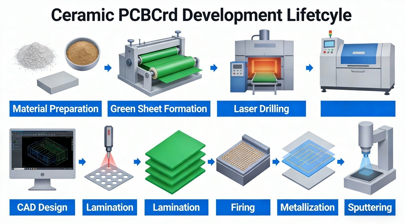
Stage 1: Thermal Simulation & Material Selection
Before a single laser is fired, we encourage our partners to utilize our Design Guide.
- Alumina ($96\% Al_2O_3$): The cost-effective workhorse ($24~W/m\cdot K$). Ideal for general automotive sensors and industrial lighting.
- Aluminium Nitride ($AlN$): The premium choice ($170+~W/m\cdot K$). Essential for high-frequency RF applications and aerospace modules where heat dissipation is critical.
Stage 2: The DPC Process (Direct Plated Copper)
Unlike the traditional etching used in FPC development, BST Ceramic PCB utilizes vacuum sputtering technology.
- Sputtering: Titanium and Copper seed layers are sputtered onto the bare ceramic in a vacuum chamber. This creates a bond strength ($>45 MPa$) far superior to the adhesives used in standard PCB fabrication.
- Plating: We thicken the copper tracks using electrolytic plating to handle high currents (up to $500\mu m$ thickness).
- Grinding: The surface is mechanically polished to ensure a flatness crucial for wire bonding—a standard often demanded by UK defence contractors.
Stage 3: Surface Finish & ISO Verification
We apply finishes such as ENIG (Electroless Nickel Immersion Gold) or ENEPIG to prevent oxidation, critical for the humid UK climate. Every board undergoes E-Testing and Automatic Optical Inspection (AOI), adhering to IPC-6012 Class 3 requirements.
Critical Applications: Aerospace, Automotive, and Renewables
The UK is a global leader in specific high-value industries. Here is how Ceramic PCB Development is solving pain points in these sectors:
1. Automotive & Motorsport (The "Motorsport Valley")
From Oxfordshire's Formula 1 teams to the burgeoning EV sector in the West Midlands, thermal management is king.
- The Challenge: Inverters in electric vehicles generate immense heat spikes during acceleration. Standard PCBs warp, leading to IGBT failure.
- The Ceramic Solution: $Si_3N_4$ (Silicon Nitride) and $AlN$ substrates handle the mechanical vibration of the track and the thermal load of the battery pack simultaneously.
2. Aerospace & Satellite Communications
With the UK Space Agency expanding its launch capabilities, the demand for "space-grade" electronics is rising.
- The Challenge: Vacuum environments offer no convection cooling. Heat must be conducted away through the board itself.
- The Ceramic Solution: An Aluminium Nitride board acts as a structural heat sink, protecting sensitive RF amplifiers without the weight of heavy metal heat spreaders.
3. Renewable Energy (Offshore Wind)
-
The Challenge: Turbines in the North Sea face salt spray and high-voltage switching loads.
-
The Ceramic Solution: Ceramic’s high dielectric breakdown voltage ($>15 kV/mm$) and zero moisture absorption make it the only viable choice for long-term reliability in power conversion modules.
Check our Product Application Gallery to see real-world examples of these technologies in action.
Why UK Innovators Choose BST Ceramic PCB
Sourcing advanced substrates can be a logistical headache for UK procurement managers. Local manufacturing often comes with prohibitive tooling costs, while generic overseas suppliers fail to meet the IPC Class 3 standards required by British engineering firms.
BST Ceramic PCB bridges this gap. We are not just a manufacturer; we are your development partner.
The BST Advantage for the UK Market:
- Rapid Prototyping: We understand the "Sprint" culture of UK tech. We offer expedited prototype runs for Ceramic PCBs, moving from file to fabrications in as little as 5 days.
- Cost-Effective Scalability: Transitioning from an R&D prototype to mass production is seamless. Our facility in China operates under ISO9001:2015, delivering British-grade quality at a competitive price point.
- Technical Consultation: We don't just print; we advise. If your current design uses FPC but fails thermally, we will guide your engineers on converting the Gerber files to a Ceramic DPC layout.
Ready to elevate your project's reliability?
Stop compromising with standard materials. Join the leading UK tech firms who trust their thermal management to us.
- Get Your Instant Quote Today – Receive a technical review within 24 hours.
- Explore Our Materials – Download the datasheet for AlN and Alumina.
Let’s build the future of UK electronics, one layer at a time.
 Products
 About us
 Contact us


