ENEPIG Surface Finish: ENEPIG vs ENIG, Plating Thickness & ENEPIG PCB Manufacturing
If you are searching for a reliable enepig ceramic pcb manufacturer, Bstceramic can be your first choice. Our engineering team focuses on high-reliability enepig solutions that improve solderability, wire bonding stability, and long-term durability. This guide explains enepig plating, compares enepig vs enig, and shows how to control enepig plating thickness from a practical engineering perspective.
Why Choose Bstceramic as Your ENEPIG Ceramic PCB Manufacturer?
Bstceramic is positioned as a one-stop PCBA service provider, built to better understand the needs of engineers. We support projects from prototype to mass production with full manufacturing traceability and engineering assistance.
- Free DFM and process adaptation suggestions
- 20 years serving 1800+ customers and 10,000+ engineers
- One-Stop Service: PCB, component sourcing, PCBA, testing & box-build
- NO MOQ with personalized support
- ISO9001/13458, IATF16949, AS9100D certified
- MES system and full traceability
- 1.5-week rapid PCBA delivery
- Strong R&D and engineering know-how
- Prototype and small volume welcome
- Quick turnaround with on-time delivery
Bstceramic provides rigid, HDI, RF, and high-speed PCB manufacturing with turnkey assembly services. All products follow IPC manufacturing standards and are designed for demanding industries.
What is the Meaning of ENEPIG?
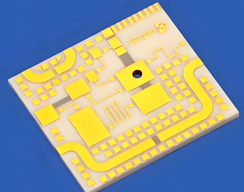
ENEPIG stands for Electroless Nickel Electroless Palladium Immersion Gold. It is a multilayer surface finish widely used on advanced enepig pcb designs where soldering and wire bonding must coexist.
The structure includes a nickel barrier layer, a palladium protection layer, and a thin immersion gold finish. Nickel ensures structural strength, palladium prevents corrosion and improves bonding, while gold protects the surface from oxidation.
Engineers prefer enepig plating because it reduces black pad risks, improves assembly reliability, and supports fine-pitch components. It is commonly used in AI servers, RF modules, automotive electronics, and medical devices.
How Does ENEPIG Plating Work in PCB Manufacturing?
ENEPIG plating is a chemical deposition process applied after copper surface preparation. Each layer is deposited sequentially to achieve uniform coverage and controlled thickness.
Typical process flow including:
- Cleaning and micro-etching
- Electroless nickel deposition
- Palladium deposition
- Immersion gold coating
This multilayer structure improves corrosion resistance and provides stable electrical contact. Compared to traditional finishes, ENEPIG offers better performance for mixed assembly processes.
ENEPIG vs ENIG: Which Surface Finish is Better for Advanced PCB?
Choosing between enepig vs enig depends on reliability targets and assembly requirements. ENEPIG introduces an additional palladium layer, which enhances bonding and reduces surface defects.
|
Feature |
ENEPIG PCB |
ENIG PCB |
|
Layer Structure |
Ni/Pd/Au |
Ni/Au |
|
Wire Bonding |
Excellent |
Limited |
|
Black Pad Risk |
Very Low |
Medium |
|
Cost |
Higher |
Lower |
|
Fine Pitch Support |
Excellent |
Good |
|
Reliability |
High-end electronics |
General use |
ENEPIG is often selected for high-reliability systems where multiple assembly processes are required, while ENIG remains suitable for cost-sensitive applications.
What is the difference between ENEPIG and Soft Gold?
ENEPIG plating and soft gold serve different engineering purposes. ENEPIG focuses on solderability and bonding flexibility, while soft gold is designed for mechanical contact surfaces such as connectors.
|
Property |
ENEPIG Plating |
Soft Gold |
|
Hardness |
Medium |
Soft |
|
Contact Durability |
Moderate |
High for insertion cycles |
|
Gold Thickness |
Thin |
Thick |
|
Application |
HDI PCB, BGA pads |
Edge connectors |
Soft gold is preferred when repeated mechanical contact is required. ENEPIG pcb is better suited for dense electronic assemblies and mixed soldering processes.
How thick is the gold in ENEPIG?
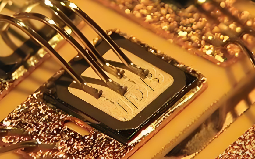
Gold thickness in enepig plating is intentionally thin because its main function is protection rather than structural reinforcement.
Typical thickness ranges:
- Nickel: 3–6 µm
- Palladium: 0.05–0.15 µm
- Gold: 0.03–0.1 µm
Thin gold reduces cost while maintaining excellent conductivity and solderability. Controlling enepig plating thickness ensures consistent assembly results and reliable long-term performance.
Why Are Engineers Switching from ENIG to ENEPIG PCB?
Many engineers move toward enepig pcb solutions because they provide greater process flexibility and reliability.
Advantages include:
- Better compatibility with wire bonding
- Reduced corrosion risk
- Stable solder joints for lead-free processes
- Improved performance in HDI structures
Applications driving adoption include AI servers, automotive ADAS systems, and high-frequency communication boards.
ENEPIG PCB Design Guidelines for Beginners
Designing for enepig plating requires understanding pad geometry and plating interactions. Beginners should focus on consistent copper thickness and correct solder mask expansion.
Recommended practices:
- Maintain uniform pad layout
- Avoid excessive copper imbalance
- Plan plating thickness early during stackup design
These considerations help ensure stable enepig plating quality and minimize assembly defects.
ENEPIG Plating Thickness Control & Process Parameters
Process control plays a major role in surface finish reliability. Engineers often monitor bath chemistry, temperature stability, and deposition timing.
|
Parameter |
Typical Value |
|
Nickel Thickness |
3–6 µm |
|
Palladium Thickness |
0.05–0.15 µm |
|
Gold Thickness |
0.03–0.1 µm |
|
Surface Roughness |
<0.3 µm |
|
Shelf Life |
12 months |
Proper thickness control improves solderability and ensures consistent electrical performance across batches.
Why Is ENEPIG More Expensive?
ENEPIG plating includes additional chemical processes and palladium materials, which increase manufacturing cost.
Main factors affecting pricing:
- Palladium layer deposition
- Additional inspection steps
- Tight process control requirements
Cost can be optimized by applying ENEPIG selectively on critical pads instead of the entire board surface.
What Applications Benefit Most from ENEPIG PCB?
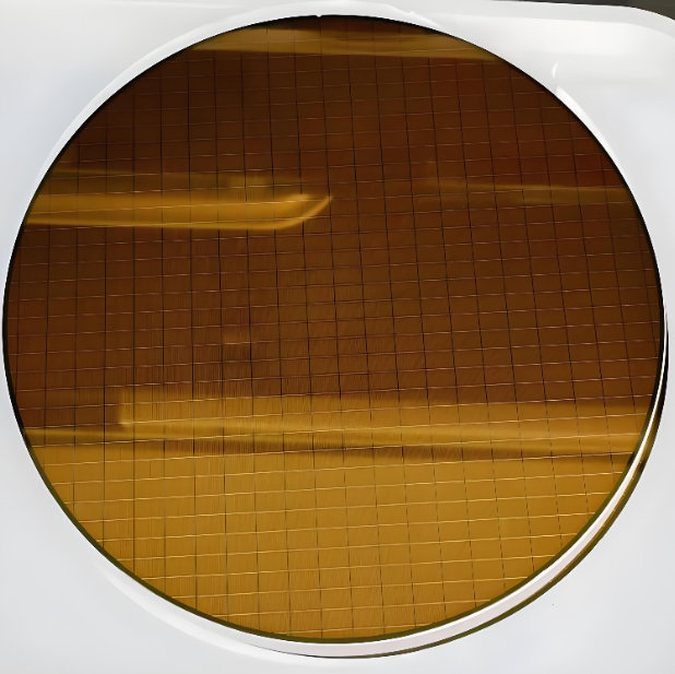
ENEPIG plating is widely used in industries that require both soldering reliability and bonding capability.
Typical applications:
- Aerospace electronics
- Medical devices
- Automotive radar systems
- High-speed computing boards
These industries benefit from ENEPIG’s stable performance and long-term reliability.
FAQs
What does Bstceramic Circuit do?
Bstceramic Circuit provides one-stop ceramic PCBA services including ceramic PCB fabrication, assembly, testing, and full electronic manufacturing solutions.
Does Bstceramic Circuit welcome prototypes or small-quantity orders?
Yes, prototype and small-batch projects are supported with engineering assistance.
Do you offer quick turn production?
Yes, rapid PCBA delivery is available depending on design complexity.
Are your PCBs RoHS and REACH compliant?
All products follow global environmental compliance and IPC standards.
Can you produce IPC Class 3 ENEPIG PCB?
Yes, high-reliability manufacturing is available for aerospace and medical applications.
What files are needed for a quotation?
Gerber files, stackup details, and surface finish requirements are required.
Order Reliable ENEPIG PCB from Bstceramic Today
If your project requires professional enepig solutions, Bstceramic offers advanced enepig pcb manufacturing and assembly services with strong engineering support. As a one-stop PCBA provider, we help engineers improve reliability and accelerate product development.
We provide enepig products tailored to your needs. If you want to place an order or request a quotation, please contact Bstceramic at sales@bstceramicpcb.com. Our team is ready to support your next project.
























 HOME
HOME


