


 HOME
HOME

-

Ceramic PCB Development: Engineering Resilience for the UK's High-Tech Future
2026 01,30 -
Automotive-grade Aluminum Nitride Substrate in Europe — Technical Specifications, Applications, and Supplier Selection
2026 01,23 -
Ceramic PCB Solutions in Sweden: Technical Requirements, Industry Applications, and Supplier Selection Strategy
2026 01,21 -
Ceramic Substrate Custom Solutions for Poland’s High-Tech Sectors: Engineering Precision & Thermal Efficiency
2026 01,20 -
High-Temperature Resistant Ceramic PCB Solutions for Industrial LTCC and HTCC Applications
2026 01,15 -
Ceramic Circuit Board Design for the UK Electronics Industry
2026 01,13 -
Aluminum Nitride (AlN) Circuit Boards: Revolutionizing Thermal Management in UK Energy Storage Systems
2026 01,10 -
Top Tips for Advanced Semiconductor Packaging Substrate Design
2026 01,05 -
Automotive electronic ceramic circuits make cars smarter and safer
2026 01,05 -
Ceramic PCB for Power Modules (IGBT): The Ultimate High-Thermal Management Guide
2025 12,27 -
Ceramic Substrate or Aluminum PCB for High-Power LEDs
2025 12,24 -
The Ultimate Guide to Alumina Circuit Board (Al2O3): High-Performance Ceramic PCB Solutions for Global Electronics
2025 12,22 -
DBC Welding Strength Compared to Other Materials
2025 12,19 -
LTCC PCB Surprises: What Most People Miss
2025 12,09 -
Comparison of DBC PCBs and MCPCBs for Cooling Performance
2025 12,03 -
Step-by-Step Guide to DPC PCB Design for Sensor Systems
2025 12,03 -
Ceramic PCBs Essential Benefits and Applications
2025 12,01 -
How Al2O3 DPC Ceramic Substrate PCB Enhances Heat Dissipation in Modern Electronics?
2025 11,28 -
How to Choose Between Ceramic, FR4, and Metal Core PCBs
2025 11,27 -
DPC Ceramic PCB Materials: Surprising Science Inside
2025 11,26 -
Wire bondable 2-layer Alumina substrates PCB | Bstceramic PCB
2025 09,22 -
Silicon Nitride Substrate, Silicon Nitride Ceramic Substrate Formula
2025 05,08 -
How to choose the appropriate substrate for ceramic circuit boards?
2023 11,16 -
Laser Cutting or Water Saw Cutting? How To Choose the Best Cutting Solution for Ceramic Circuit Boards
2023 11,13 -
Why Ceramic PCB Is So Expensive?
2023 11,10 -
Which Process Ceramic Circuit Board Is A Better Solution For Semiconductor Refrigerator Chips?
2023 11,06 -
Silicon Printing Circuit Boards For Advancing Electronics
2023 10,27 -
What is the Difference Between HTCC and LTCC Ceramic PCB
2023 10,06 -
What is the Difference Between 96% and 99% Aluminum Oxide in Ceramic PCBs?
2023 09,20 -
Why thick film ceramic PCB is good for oil level sensor in automotive industry?
2023 08,25 -
Silver Paste: The Best Conductor Material for Via Holes in Thick Film Ceramic Boards
2023 08,16 -
Testing Circuit Board Ceramic Diode Fuses: A Complete Guide
2023 08,07 -
Why DBC is replaced by DPC in ceramic PCB manufacturing?
2023 08,01 -
What is thick film ceramic PCB?
2023 08,02
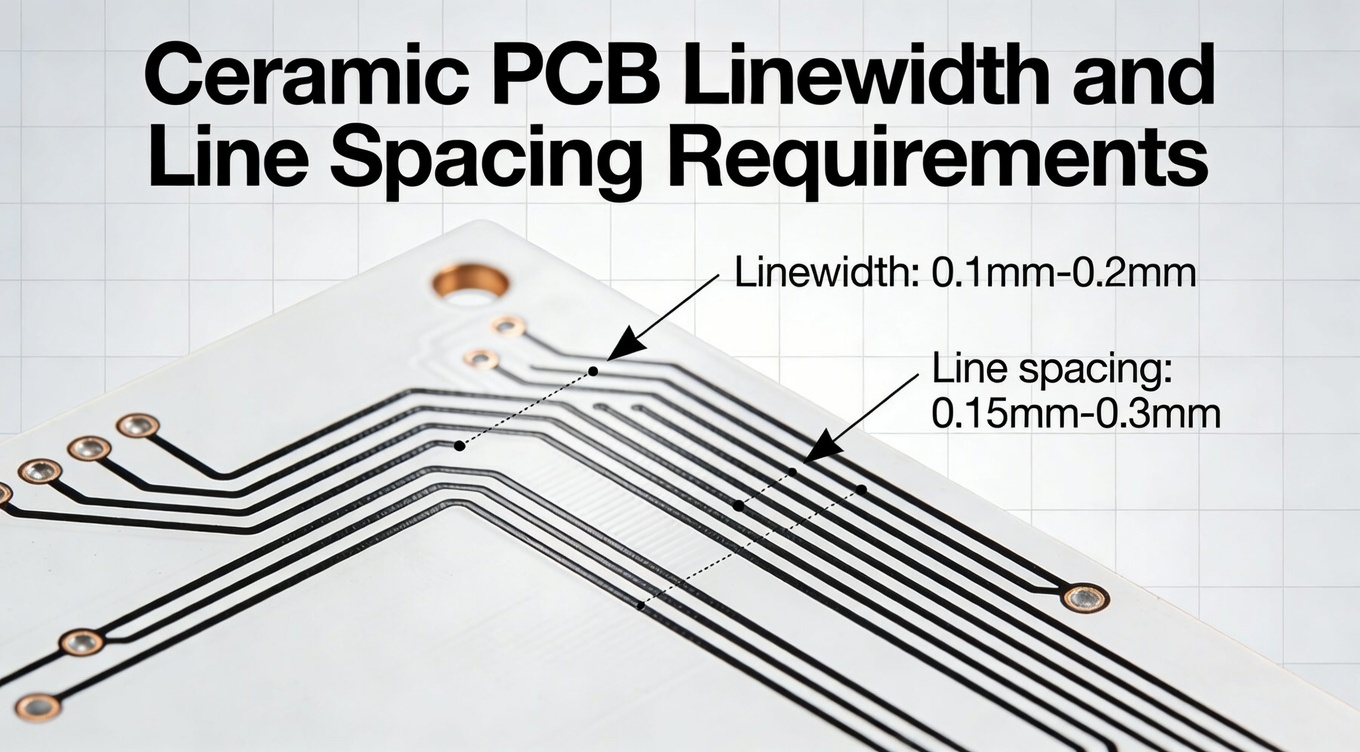
Ceramic PCB Linewidth and Line Spacing
Technical Standards, Industry Requirements and Precision Manufacturing Solutions Introduction
As Germany continues to lead Europe in advanced manufacturing, automotive electronics, industrial automation, and high-reliability power systems, ceramic PCBs are playing an increasingly critical role. Compared with traditional FR-4 boards, ceramic substrates such as alumina (Al₂O₃) and aluminum nitride (AlN) offer superior thermal conductivity, electrical insulation, and dimensional stability.
Within ceramic PCB design and fabrication, linewidth and line spacing are among the most decisive technical parameters. They directly influence electrical performance, thermal behavior, reliability, and manufacturability. For German OEMs and Tier-1 suppliers, where compliance, repeatability, and process transparency are essential, understanding and controlling these parameters is not optional—it is a baseline requirement.
This article provides an in-depth analysis of ceramic PCB linewidth and line spacing requirements for the German market, integrating European and German standards, industry-specific expectations, and proven manufacturing strategies. It also explains how BSTCERAMICPCB supports German customers with precision ceramic PCB solutions from design to mass production.
Understanding Linewidth and Line Spacing in Ceramic PCB Design
In ceramic PCB technology, linewidth refers to the width of the conductive trace deposited on the ceramic substrate, while line spacing defines the minimum distance between adjacent conductive features. Although these concepts are familiar to PCB engineers, their implications are fundamentally different when applied to ceramic materials.
Unlike organic laminates, ceramic substrates are rigid, brittle, and processed using metallization techniques such as thick-film printing, DBC (Direct Bonded Copper), or AMB (Active Metal Brazing). Each process imposes specific limits on how fine or wide traces can be produced consistently. In Germany’s high-precision electronics environment, these limits must be clearly understood during the design phase.
From a functional perspective, linewidth and line spacing affect:
- Current-carrying capacity, especially in power and automotive applications
- Electrical insulation and creepage distance, critical for safety compliance
- Signal integrity, particularly in high-frequency and control circuits
- Thermal distribution, as copper geometry influences heat spreading
German manufacturers typically demand predictable, repeatable results rather than aggressive minimum features. Therefore, optimal ceramic PCB design often balances electrical requirements with process robustness and yield stability, rather than pushing theoretical limits.
Technical Requirements and Industry Standards in Germany
Germany follows a combination of international IPC standards, European norms, and industry-specific regulations when defining acceptable linewidth and line spacing for ceramic PCBs.
From a general perspective, IPC-6012 and IPC-2221 provide baseline guidance for conductor geometry, spacing, and insulation. However, in ceramic PCB applications, these guidelines are often adapted to account for ceramic-specific properties such as thermal expansion mismatch and metallization adhesion strength.
German standards and practices typically emphasize:
- Electrical clearance and creepage under high voltage
- Long-term reliability under thermal cycling
- Dimensional stability over extended operating lifetimes
In many German industrial and automotive projects, conservative spacing rules are preferred. For example, while a ceramic PCB process may technically support very fine spacing, German OEMs often specify larger margins to ensure compliance with VDE, IEC, or customer-specific reliability requirements.
Material selection also directly impacts achievable geometry. Alumina substrates generally allow stable, medium-fine linewidths suitable for industrial control and sensor electronics. Aluminum nitride, with its higher thermal conductivity, is often used in power electronics but requires stricter process control to maintain consistent line definition.
At BSTCERAMICPCB, linewidth and spacing capabilities are clearly defined during DFM review, ensuring that German customers receive realistic, production-proven design rules rather than laboratory-only values.
Ceramic PCB Linewidth and Line Spacing Requirements by Industry in Germany
Automotive Electronics
Germany’s automotive sector places extremely high demands on ceramic PCB reliability. In applications such as power modules, sensors, and control units, linewidth and line spacing must support:
- High current density
- Long-term vibration resistance
- Compliance with ISO 26262 functional safety requirements
Automotive ceramic PCBs typically prioritize robust copper geometry over ultra-fine features. Wider traces and sufficient spacing reduce the risk of micro-cracking, delamination, or insulation degradation during thermal cycling.
Industrial Automation and Power Electronics
Industrial drives, inverters, and control systems often operate continuously under elevated temperatures. In these cases, linewidth is closely linked to thermal dissipation, while line spacing ensures safe operation under high voltage.
German industrial customers frequently request conservative spacing values combined with thick copper layers to achieve stable performance over decades of service life.
Telecommunications and High-Frequency Modules
For RF and communication equipment, signal integrity becomes a dominant factor. Controlled impedance traces, consistent linewidth, and precise spacing are essential to minimize signal loss and interference.
Ceramic substrates offer excellent dielectric stability, but achieving tight tolerances requires close collaboration between design engineers and manufacturers. BSTCERAMICPCB supports this process through early-stage design consultation and prototype validation.
Medical and Precision Electronics
Medical devices in Germany are governed by strict regulatory frameworks. Ceramic PCBs used in imaging, diagnostics, or monitoring equipment must demonstrate both electrical precision and manufacturing repeatability.
Here, linewidth and spacing decisions are driven by reliability and certification readiness rather than cost optimization.
Design Tradeoffs and Best Practices for High-Precision Ceramic PCBs
Designing ceramic PCBs for the German market requires careful tradeoffs. Narrow linewidths may enable compact layouts, but they also increase process sensitivity. Similarly, minimal spacing can improve density but may compromise insulation reliability under high voltage or humidity.
Best practices include:
- Selecting linewidths that align with proven manufacturing windows
- Allowing sufficient spacing for voltage and environmental conditions
- Considering metallization thickness and surface finish effects
- Performing DFM reviews before finalizing layouts
German customers increasingly value design for manufacturability (DFM) as part of supplier evaluation. A ceramic PCB supplier is expected not only to fabricate boards but also to provide engineering feedback that improves yield and reliability.
BSTCERAMICPCB integrates DFM analysis into every project, helping German clients optimize linewidth and spacing based on real production data rather than assumptions.
Why German Customers Choose BSTCERAMICPCB
For German OEMs and EMS providers, supplier selection is based on technical credibility, transparency, and long-term stability. BSTCERAMICPCB has built its ceramic PCB manufacturing process to align with these expectations.
Key advantages include:
- Clearly defined linewidth and line spacing capabilities for different ceramic processes
- Engineering-led communication with detailed DFM feedback
- Stable production processes for alumina and aluminum nitride substrates
- Quality inspection systems designed to meet European reliability expectations
By combining material expertise, process control, and application-level understanding, BSTCERAMICPCB supports German customers from prototype development to volume production.
For companies seeking reliable ceramic PCB linewidth and line spacing solutions tailored to German industry standards, partnering with an experienced manufacturer reduces risk, shortens development cycles, and improves long-term product performance.
Conclusion and Next Steps
As Germany continues to demand higher reliability, precision, and compliance in electronic systems, ceramic PCB linewidth and line spacing will remain a critical design and manufacturing focus. Understanding how these parameters interact with materials, processes, and industry standards is essential for successful projects.
BSTCERAMICPCB offers German customers a proven path to precision ceramic PCB manufacturing, combining technical depth with practical production experience.
 Products
 About us
 Contact us


