


 HOME
HOME

-

Ceramic PCB Development: Engineering Resilience for the UK's High-Tech Future
2026 01,30 -
Ceramic PCB for Power Modules (IGBT) in Australia — Technical Standards, Thermal Solutions, and Supplier Strategy
2026 01,23 -
Automotive-grade Aluminum Nitride Substrate in Europe — Technical Specifications, Applications, and Supplier Selection
2026 01,23 -
Ceramic PCB Solutions in Sweden: Technical Requirements, Industry Applications, and Supplier Selection Strategy
2026 01,21 -
Ceramic Substrate Custom Solutions for Poland’s High-Tech Sectors: Engineering Precision & Thermal Efficiency
2026 01,20 -
High-Temperature Resistant Ceramic PCB Solutions for Industrial LTCC and HTCC Applications
2026 01,15 -
Ceramic Circuit Board Design for the UK Electronics Industry
2026 01,13 -
BST Ceramic PCB Expands Small Batch Ceramic PCB Manufacturing Support for Swiss High-Precision Electronics
2026 01,13 -
Aluminum Nitride (AlN) Circuit Boards: Revolutionizing Thermal Management in UK Energy Storage Systems
2026 01,10 -
Top Tips for Advanced Semiconductor Packaging Substrate Design
2026 01,05 -
Automotive electronic ceramic circuits make cars smarter and safer
2026 01,05 -
The Ultimate Guide to Ceramic PCB Air Tightness: Ensuring Hermetic Reliability for High-Performance Electronics in North America
2025 12,29 -
Ceramic PCB for Power Modules (IGBT): The Ultimate High-Thermal Management Guide
2025 12,27 -
Ceramic Substrate or Aluminum PCB for High-Power LEDs
2025 12,24 -
The Ultimate Guide to Alumina Circuit Board (Al2O3): High-Performance Ceramic PCB Solutions for Global Electronics
2025 12,22 -
DBC Welding Strength Compared to Other Materials
2025 12,19 -
LTCC PCB Surprises: What Most People Miss
2025 12,09 -
Comparison of DBC PCBs and MCPCBs for Cooling Performance
2025 12,03 -
Step-by-Step Guide to DPC PCB Design for Sensor Systems
2025 12,03 -
Ceramic PCBs Essential Benefits and Applications
2025 12,01 -
How Al2O3 DPC Ceramic Substrate PCB Enhances Heat Dissipation in Modern Electronics?
2025 11,28 -
How to Choose Between Ceramic, FR4, and Metal Core PCBs
2025 11,27 -
DPC Ceramic PCB Materials: Surprising Science Inside
2025 11,26 -
Wire bondable 2-layer Alumina substrates PCB | Bstceramic PCB
2025 09,22 -
Silicon Nitride Substrate, Silicon Nitride Ceramic Substrate Formula
2025 05,08 -
How to choose the appropriate substrate for ceramic circuit boards?
2023 11,16 -
Laser Cutting or Water Saw Cutting? How To Choose the Best Cutting Solution for Ceramic Circuit Boards
2023 11,13 -
Why Ceramic PCB Is So Expensive?
2023 11,10 -
Which Process Ceramic Circuit Board Is A Better Solution For Semiconductor Refrigerator Chips?
2023 11,06 -
Silicon Printing Circuit Boards For Advancing Electronics
2023 10,27 -
What is the Difference Between HTCC and LTCC Ceramic PCB
2023 10,06 -
What is the Difference Between 96% and 99% Aluminum Oxide in Ceramic PCBs?
2023 09,20 -
Why thick film ceramic PCB is good for oil level sensor in automotive industry?
2023 08,25 -
Statistical analysis of ceramic PCB application fields
2023 08,16 -
Notice of anti-static requirements for PCBA processing and production
2023 08,16 -
Silver Paste: The Best Conductor Material for Via Holes in Thick Film Ceramic Boards
2023 08,16 -
Testing Circuit Board Ceramic Diode Fuses: A Complete Guide
2023 08,07 -
Why DBC is replaced by DPC in ceramic PCB manufacturing?
2023 08,01 -
What is thick film ceramic PCB?
2023 08,02
Thick Film Ceramic PCB: A Practical Manufacturing Guide for High-Reliability Electronics
What Is a Thick Film Ceramic PCB and Why Is It Used in Electronics?
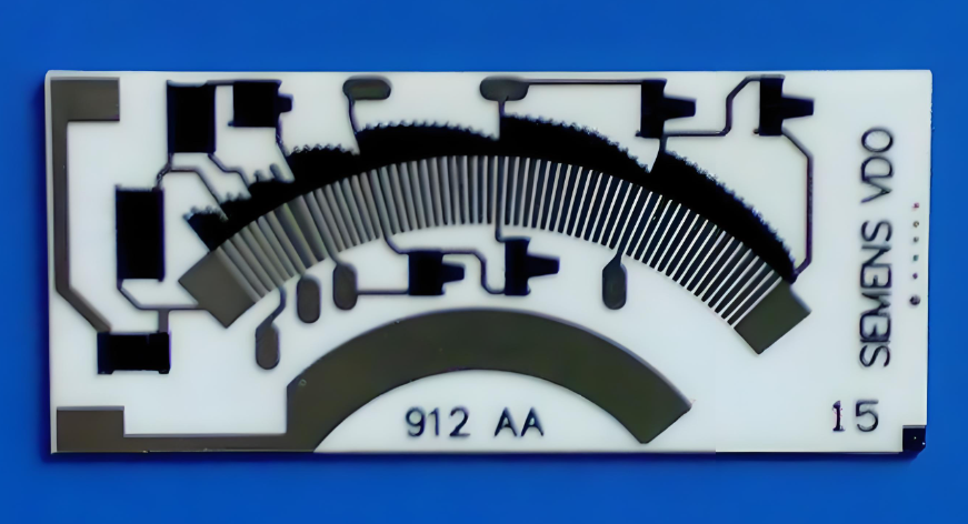
A thick film ceramic PCB is a ceramic circuit board made by screen-printing conductive, resistive, and dielectric pastes onto a ceramic substrate, then firing the layers at high temperature. This creates durable circuitry bonded directly to the ceramic surface.
Engineers choose thick film ceramic PCB technology when standard FR4 cannot handle heat, vibration, or long-life requirements. It is common in industrial control, automotive electronics, medical devices, and power systems where stable performance matters.
Why Choose Bstceramic as Your Thick Film Ceramic PCB Manufacturer?
If you are sourcing a thick film ceramic PCB manufacturer, engineering support and process control matter as much as equipment. Bstceramic is built around one mission: One-stop PCBA service provider, better understanding the needs of engineers.
What practical advantages do engineers get with Bstceramic?
- Free DFM and process adaptation suggestions
- 20 years of experience, serving 1,800+ customers and 10,000+ engineers
- One-Stop Service: PCB, component sourcing, PCBA, testing, and box-building
- No MOQ, personal service, prototype & small volume welcome
- Certified systems: ISO9001, ISO13485, IATF16949, AS9100D
- MES & Traceability for full process tracking
- 1.5-week rapid PCBA delivery, quick turn-out and on-time delivery
- Technical support before and after sales, prompt feedback within 12 hours
How Does Thick Film Ceramic PCB Manufacturing Work Step by Step?
The thick film ceramic PCB manufacturing process is a repeatable sequence of printing and firing. It focuses on reliability and strong adhesion rather than ultra-fine line geometry.
Step 1: Ceramic Substrate Preparation
Most thick film ceramic PCBs use alumina (Al₂O₃) substrates, typically 96% or 99% purity. The ceramic panel is cleaned and surface-treated to ensure proper adhesion of printed pastes.
Step 2: Screen Printing of Conductive Layers
Conductive pastes, such as silver or silver-palladium, are printed through precision screens. The printed traces are relatively thick compared to thin film processes, which is where the term “thick film” comes from.
Step 3: Drying and High-Temperature Firing
After printing, the board is dried and fired in a conveyor furnace at temperatures around 850–950 °C. This firing process melts the glass components in the paste, bonding the conductor permanently to the ceramic surface.
Step 4: Multi-Layer Build-Up
If resistors or dielectric layers are required, additional pastes are printed and fired in sequence. This allows resistors, conductors, and insulation layers to coexist on the same ceramic PCB.
Step 5: Laser Trimming (Optional)
For precision resistor values, laser trimming is used to fine-tune resistance after firing. This step is common in sensor and analog circuits.
Step 6: Inspection and Electrical Testing
Final inspection includes visual checks, adhesion tests, and electrical measurements to ensure performance consistency.
This process favors robustness and repeatability rather than ultra-fine geometries.
What Materials Are Used in Thick Film Ceramic PCBs?
A thick film ceramic PCB relies on a small set of proven materials. The goal is stable adhesion, predictable electrical behavior, and long-term reliability.
Ceramic Substrates
-
Alumina (Al₂O₃)
-
96% alumina: cost-effective, widely used
-
99% alumina: higher purity, better insulation and thermal stability
-
Conductive Pastes
-
Silver (Ag): high conductivity, cost-effective
-
Silver-palladium (AgPd): improved migration resistance
-
Gold (Au): excellent stability, higher cost
Resistive Pastes
-
Ruthenium-based thick film resistors
-
Designed for laser trimming and long-term stability
Dielectric Pastes
-
Glass-based insulating materials
-
Used to isolate conductors and form multilayer structures
Each material is selected to survive repeated firing cycles without degradation.
Thick Film Ceramic PCB vs Thin Film Ceramic PCB: What Is the Real Difference?
Thick film ceramic PCB vs thin film ceramic PCB is mainly a process and capability decision. Thick film favors robustness and cost control; thin film favors ultra-fine features and higher precision.
| Item | Thick Film Ceramic PCB | Thin Film Ceramic PCB |
|---|---|---|
| Typical line width | About 100–200 micrometers | Often below 20 micrometers |
| Process | Screen printing + firing | Vacuum deposition + photolithography |
| Cost level | Lower | Higher |
| Best fit | Industrial, power, harsh environments | RF, sensors, precision micro-patterning |
Thick film ceramic PCBs focus on durability and cost control. Thin film ceramic PCBs prioritize precision and miniaturization. Engineers choose between them based on application needs rather than technology preference.
What Electrical and Thermal Performance Can Thick Film Ceramic PCBs Achieve?
A thick film ceramic PCB delivers stable electrical performance over a wide temperature range. Ceramic substrates provide excellent insulation resistance and low dielectric loss compared to organic materials.
Electrical Characteristics
-
Stable resistance values
-
Low noise for analog circuits
-
Strong adhesion prevents trace lift-off
Thermal Characteristics
-
Continuous operation at elevated temperatures
-
Efficient heat spreading through ceramic
-
No glass transition temperature limitations
Although thick film traces are not as thick as DBC copper, they handle moderate power reliably when designed correctly.
Where Are Thick Film Ceramic PCBs Commonly Used?
Thick film ceramic PCB for power electronics is a common fit when heat and reliability drive the design. It is also used in measurement and sensor assemblies where long-term stability matters.
Typical applications
- Automotive control and sensing modules
- Industrial power supplies and high-temperature electronics
- Medical monitoring and diagnostic electronics
- Sensor circuits, instrumentation, and ruggedized modules
In these applications, long-term reliability is more important than compact size.
What Are the Design Rules for Thick Film Ceramic PCB Layout?
Thick film ceramic PCB design guidelines focus on printability and firing stability. If you design like FR4, you may create yield and reliability risks.
What layout rules help improve yield?
- Avoid sharp corners in printed traces to reduce stress points
- Use smooth transitions and consistent trace widths
- Keep adequate spacing based on screen printing capability
- Plan resistor trimming zones early if resistors are printed
- Consider assembly stress and thermal expansion mismatch
What files should you prepare for DFM review?
- Gerber or manufacturing drawings for printed layers
- Stack and layer intent (conductors, dielectrics, resistor regions)
- Bill of materials and assembly constraints if PCBA is required
- Test requirements and acceptance criteria (IPC Class 2 or higher when needed)
What Are the Main Advantages and Limitations of Thick Film Ceramic PCBs?
A thick film ceramic PCB is attractive because it is robust and cost-efficient for many harsh-environment designs. It is not intended for very dense routing or the smallest feature sizes.
Advantages
- Strong adhesion and long-term reliability
- Good thermal stability and temperature resistance
- Cost-effective versus thin film solutions
- Suitable for printed resistors and hybrid functions
Limitations
- Lower routing density than thin film or advanced organic HDI
- Feature size and spacing are limited by screen printing
- Not the best first choice for ultra-high-frequency RF micro-structures
How Does Thick Film Ceramic PCB Compare with DBC and DPC Ceramic Boards?
Thick film ceramic PCB vs DBC vs DPC is a common selection question. Thick film targets moderate power with strong cost control, while DBC is often chosen for very high power and heat flow.
| Technology | Metallization | Power Handling | Relative Cost | Best Use Cases |
|---|---|---|---|---|
| Thick Film Ceramic PCB | Printed paste conductors | Medium | Lower | Industrial electronics, sensors, moderate power modules |
| DPC Ceramic | Plated copper on ceramic | Medium to high | Medium | Fine features with better copper performance |
| DBC Ceramic | Bonded thick copper | High to very high | Higher | Power modules, inverters, high thermal load designs |
How Much Does a Thick Film Ceramic PCB Cost and What Affects Pricing?
Thick film ceramic PCB cost is mainly driven by substrate size, paste type, layer count, and inspection level. Clear specifications reduce cost surprises and shorten quoting cycles.
What factors raise or lower cost?
- Substrate material and thickness (96% vs 99% alumina)
- Conductor paste choice (Ag vs Au)
- Number of print-and-fire cycles and total layers
- Laser trimming needs for resistor tolerance
- Electrical tests, special inspections, and traceability level
How to reduce cost without sacrificing reliability?
- Use standardized sizes when possible
- Define critical tolerances only where needed
- Request DFM early to avoid redesign loops
- Align test coverage with application risk level
Thick Film Ceramic PCB FAQs
1. What is the typical MOQ for thick film ceramic PCB prototyping?
Thick film ceramic PCB prototyping often supports low MOQ because screen printing is flexible for small batches. Bstceramic also welcomes prototypes and small volume orders, so you can validate designs before scaling.
2. Can thick film ceramic PCB boards run at high temperature for long periods?
Yes. Ceramic substrates remain stable at elevated temperatures and do not have a glass transition behavior like FR4. This is a key reason thick film ceramic circuits are used in harsh environments.
3. Is a thick film ceramic PCB suitable for power electronics?
Yes, for moderate power density applications where stable performance and heat tolerance are required. For very high power modules, DBC may be more suitable, which is why comparing requirements early is important.
4. What files do you need to quote thick film ceramic PCB fabrication?
Gerber files or layer drawings for printed patterns are the most important. For turnkey PCBA, you should also provide a BOM, placement data, and any test requirements so the quote is accurate.
5. Does Bstceramic provide engineering assistance and DFM support?
Yes. We provide Free DFM and process adaptation suggestions. This helps beginners avoid common printability and assembly risks before production begins.
6. Do you offer quick turn production and on-time delivery?
Yes. We support quick turn-out and on-time delivery, including a 1.5-week rapid PCBA option for urgent schedules. Production is supported by MES & Traceability controls to keep outputs consistent.
Work with Bstceramic for Thick Film Ceramic PCB Manufacturing
Bstceramic is a reliable partner for thick film ceramic PCB manufacturing, combining ceramic process experience with strong engineering support. We help beginners move from concept to verified hardware with fewer iterations and clearer process boundaries.
If you need a thick film ceramic PCB or related ceramic PCB solutions, place your order by contacting us at sales@bstceramicpcb.com. Bstceramic is ready to support your prototype, small batch, and production builds with practical engineering guidance.
 Products
 About us
 Contact us


