What Is a DBC Ceramic PCB and How Does Direct Bonded Copper Technology Work?
DBC ceramic PCB technology has become a preferred solution for high-power electronic applications where thermal reliability, electrical insulation, and mechanical strength must work together. Unlike conventional laminates, DBC structures combine copper and ceramic through a direct bonding process that creates an exceptionally stable interface. Engineers working on EV inverters, IGBT modules, or high-current power devices often choose DBC substrates when heat density and electrical performance exceed the limits of standard materials.
In this article, you will learn how DBC ceramic PCB works, which materials are commonly used, how the manufacturing process is structured, and what design considerations influence performance and cost. The goal is to provide a clear engineering perspective so readers can evaluate DBC technology with confidence before moving into real production.
What Is a DBC Ceramic PCB and How Does Direct Bonded Copper Technology Work?
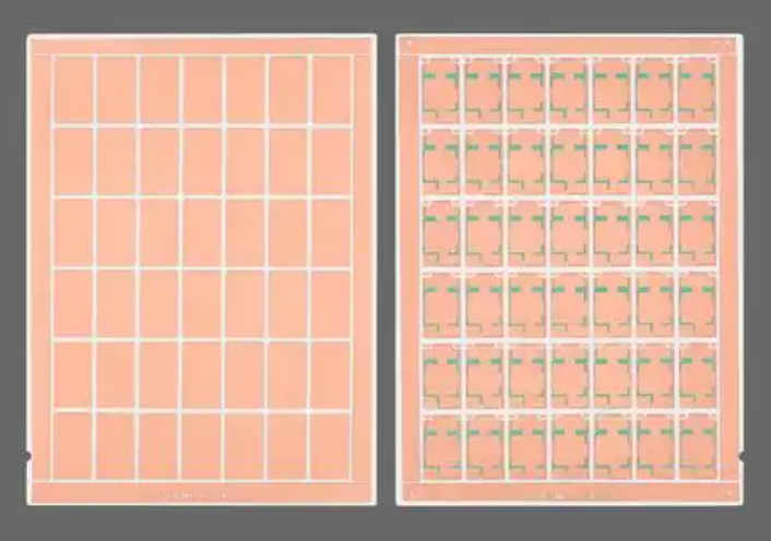
A DBC ceramic PCB is a copper-ceramic substrate created by bonding pure copper foil directly onto a ceramic surface at high temperature. During this process, copper oxidizes slightly and forms a eutectic layer that chemically bonds to the ceramic base. This differs from plated or laminated structures because the bond is metallurgical rather than adhesive.
The direct bonding mechanism provides several engineering advantages:
- Extremely strong copper adhesion to ceramic
- High thermal conductivity across the interface
- Low thermal resistance compared to plated copper
- Excellent dimensional stability under temperature cycling
Because the copper layer is thick and mechanically robust, DBC boards are often used as both circuit substrate and heat spreader within power modules.
Why Is DBC Ceramic PCB Used in High-Power Electronics Instead of FR-4?
FR-4 remains common for signal and control boards, but high-power systems introduce challenges that organic substrates cannot easily handle. As current density rises, the ability to dissipate heat becomes critical.
DBC ceramic PCB offers several benefits compared with FR-4:
- Much higher thermal conductivity
- Minimal coefficient of thermal expansion mismatch with semiconductor dies
- Superior insulation performance at elevated temperature
- Greater long-term reliability in harsh environments
In applications such as traction inverters or motor drives, engineers often transition from FR-4 to ceramic when thermal hotspots begin limiting design margins.
What Materials Are Used in DBC Ceramic PCB?
Material selection directly affects thermal performance, mechanical strength, and overall cost. The most common ceramic bases used in DBC construction include alumina (Al₂O₃), aluminum nitride (AlN), and silicon nitride (Si₃N₄).
Al₂O₃ (Alumina)
Widely used due to its stable insulation properties and cost efficiency. Typical thermal conductivity ranges around 24 W/m·K. Suitable for moderate power density applications.
AlN (Aluminum Nitride)
Offers significantly higher thermal conductivity, often exceeding 170 W/m·K. Ideal for high-frequency power modules or LED drivers requiring rapid heat spreading.
Si₃N₄ (Silicon Nitride)
Known for exceptional mechanical toughness and thermal shock resistance. Frequently chosen for automotive and EV modules where vibration and reliability are critical.
Choosing between these materials requires balancing thermal requirements, mechanical stress tolerance, and budget constraints.
How Does the Manufacturing Process of DBC Ceramic PCB Work Step by Step?
The production flow of DBC ceramic PCB combines ceramic processing with copper patterning techniques. While details vary between manufacturers, the general process includes:
- Ceramic substrate preparation and surface treatment
- Oxidation of copper foil to enable eutectic bonding
- High-temperature bonding of copper to ceramic
- Photolithography and etching to form circuit patterns
- Surface finishing such as ENIG or silver plating
- Final inspection and electrical testing
Because the copper layer is thick, etching parameters and line definition require precise control. Process stability strongly influences yield, especially when designing narrow traces or heavy copper layouts.
Key Advantages of DBC Ceramic PCB
Thermal performance is one of the main reasons engineers adopt DBC substrates. The ceramic base acts as an insulator while the bonded copper spreads heat efficiently across the board.
Key thermal advantages include:
- Direct heat conduction from semiconductor die to copper plane
- Reduced thermal resistance compared with multilayer laminates
- High operating temperature capability
- Improved reliability during thermal cycling
These properties allow designers to reduce heatsink size or increase power density without compromising safety margins.
DBC Ceramic PCB vs AMB vs Thick Film Ceramic PCB — Which Is Better?
Different ceramic PCB technologies address different application needs. Understanding their differences helps engineers select the right platform.
|
Technology |
Copper Structure |
Typical Use Case |
Performance Focus |
|
DBC |
Bonded thick copper foil |
Power modules, EV inverters |
Thermal conduction + current handling |
|
AMB |
Active metal brazing |
Very high power density |
Strong metallurgical bonding |
|
Thick Film |
Printed conductor paste |
Sensors, low-power electronics |
Cost efficiency |
DBC is often considered the balanced choice, offering high reliability without the complexity of AMB processes.
What Copper Thickness and Current Capacity Can DBC Ceramic PCB Handle?
One of the defining features of DBC technology is its ability to support very thick copper layers. Common copper thickness ranges from 0.3 mm up to 0.8 mm or more depending on application requirements.
Higher copper thickness allows:
- Increased current carrying capability
- Reduced resistive losses
- Better heat spreading across power traces
However, thicker copper also influences etching tolerances and design spacing, so collaboration between design engineers and fabrication teams is essential.
Where Is DBC Ceramic PCB Commonly Used? EV, IGBT, and Power Modules
DBC ceramic PCB is widely used across industries that demand robust thermal performance and electrical reliability. Typical applications include:
- Electric vehicle inverter modules
- IGBT and MOSFET power stages
- Industrial motor drives
- Renewable energy converters
- High-power LED modules
These applications benefit from the ceramic substrate’s ability to maintain performance under high temperature and continuous load.
What Design Rules Should Engineers Follow When Designing a DBC Ceramic PCB?
Designing for DBC requires a different mindset compared with standard PCB layout. Engineers should consider several factors early in the design phase:
- Maintain wider trace spacing due to thick copper etching tolerances
- Optimize copper geometry to reduce thermal stress
- Avoid sharp internal corners that concentrate mechanical stress
- Plan die attach areas with uniform copper distribution
Thermal expansion matching between components and substrate is also critical. Early DFM collaboration helps reduce costly redesign cycles.
How Much Does DBC Ceramic PCB Cost and What Affects Pricing?
DBC substrates typically cost more than traditional FR-4 boards due to material and processing complexity. Key factors affecting pricing include:
- Ceramic material type (Al₂O₃ vs AlN vs Si₃N₄)
- Copper thickness
- Pattern complexity
- Surface finish requirements
- Production volume
Although initial cost may be higher, DBC solutions often reduce system-level expenses by improving reliability and minimizing cooling requirements.
How to Choose a Reliable DBC Ceramic PCB Manufacturer?
Selecting a manufacturing partner is crucial because DBC production requires specialized equipment and process control. Engineers should evaluate suppliers based on:
- Experience with ceramic bonding technology
- Capability in thick copper patterning
- Thermal simulation and DFM support
- Quality certifications and traceability systems
- Consistent supply chain for ceramic materials
A manufacturer with strong engineering collaboration can significantly reduce development risk and accelerate product validation.
FAQs
Is DBC ceramic PCB suitable for high-frequency applications?
Yes, especially when using AlN substrates with low dielectric loss. However, layout and impedance design remain important.
Can DBC ceramic PCB support multilayer structures?
Most DBC boards are single or double layer, but hybrid designs combining DBC with other substrates are possible.
What surface finishes are commonly used on DBC copper?
ENIG, ENEPIG, and silver plating are widely used depending on assembly requirements.
Is DBC better than metal core PCB?
For extreme thermal performance and high current density, DBC generally provides better reliability.
How thick can the copper layer be?
Depending on the supplier, copper thickness can exceed 800 µm, supporting very high current paths.
In Conclusion
If your project requires a professional solution for ceramic PCB manufacturing, Bstceramic Circuit provides engineering-driven support, experienced professional talents, and dedicated project coordinators who proactively assist from design review to mass production.
With strong expertise in Al₂O₃, AlN, and Si₃N₄ DBC fabrication, the team focuses on helping customers outdo traditional limitations and bring high-power products to market with confidence.























 HOME
HOME


