


 HOME
HOME

-

AI-Driven Process Control for DPC Ceramic PCB Yield Improvement in Colombia’s Advanced Electronics Market
2026 02,28 -
Ceramic Circuit Board Quality Standards in the United States — Technical Requirements, Industry Practices, and Supplier Guide
2026 02,25 -
Ceramic PCB for LED Lighting in Colombia
2026 02,06 -
Ceramic PCB Linewidth and Line Spacing
2026 02,06 -
Ceramic PCB Development: Engineering Resilience for the UK's High-Tech Future
2026 01,30 -
Ceramic PCB for Power Modules (IGBT) in Australia — Technical Standards, Thermal Solutions, and Supplier Strategy
2026 01,23 -
Automotive-grade Aluminum Nitride Substrate in Europe — Technical Specifications, Applications, and Supplier Selection
2026 01,23 -
Ceramic PCB Solutions in Sweden: Technical Requirements, Industry Applications, and Supplier Selection Strategy
2026 01,21 -
Ceramic Substrate Custom Solutions for Poland’s High-Tech Sectors: Engineering Precision & Thermal Efficiency
2026 01,20 -
High-Temperature Resistant Ceramic PCB Solutions for Industrial LTCC and HTCC Applications
2026 01,15 -
Ceramic Circuit Board Design for the UK Electronics Industry
2026 01,13 -
Aluminum Nitride (AlN) Circuit Boards: Revolutionizing Thermal Management in UK Energy Storage Systems
2026 01,10 -
Top Tips for Advanced Semiconductor Packaging Substrate Design
2026 01,05 -
Automotive electronic ceramic circuits make cars smarter and safer
2026 01,05 -
The Ultimate Guide to Ceramic PCB Air Tightness: Ensuring Hermetic Reliability for High-Performance Electronics in North America
2025 12,29 -
Ceramic PCB for Power Modules (IGBT): The Ultimate High-Thermal Management Guide
2025 12,27 -
Ceramic Substrate or Aluminum PCB for High-Power LEDs
2025 12,24 -
The Ultimate Guide to Alumina Circuit Board (Al2O3): High-Performance Ceramic PCB Solutions for Global Electronics
2025 12,22 -
DBC Welding Strength Compared to Other Materials
2025 12,19 -
LTCC PCB Surprises: What Most People Miss
2025 12,09 -
Comparison of DBC PCBs and MCPCBs for Cooling Performance
2025 12,03 -
Step-by-Step Guide to DPC PCB Design for Sensor Systems
2025 12,03 -
Ceramic PCBs Essential Benefits and Applications
2025 12,01 -
How Al2O3 DPC Ceramic Substrate PCB Enhances Heat Dissipation in Modern Electronics?
2025 11,28 -
How to Choose Between Ceramic, FR4, and Metal Core PCBs
2025 11,27 -
DPC Ceramic PCB Materials: Surprising Science Inside
2025 11,26 -
Wire bondable 2-layer Alumina substrates PCB | Bstceramic PCB
2025 09,22 -
Silicon Nitride Substrate, Silicon Nitride Ceramic Substrate Formula
2025 05,08 -
How to choose the appropriate substrate for ceramic circuit boards?
2023 11,16 -
Laser Cutting or Water Saw Cutting? How To Choose the Best Cutting Solution for Ceramic Circuit Boards
2023 11,13 -
Why Ceramic PCB Is So Expensive?
2023 11,10 -
Which Process Ceramic Circuit Board Is A Better Solution For Semiconductor Refrigerator Chips?
2023 11,06 -
Silicon Printing Circuit Boards For Advancing Electronics
2023 10,27 -
What is the Difference Between HTCC and LTCC Ceramic PCB
2023 10,06 -
What is the Difference Between 96% and 99% Aluminum Oxide in Ceramic PCBs?
2023 09,20 -
Why thick film ceramic PCB is good for oil level sensor in automotive industry?
2023 08,25 -
Notice of anti-static requirements for PCBA processing and production
2023 08,16 -
Silver Paste: The Best Conductor Material for Via Holes in Thick Film Ceramic Boards
2023 08,16 -
Testing Circuit Board Ceramic Diode Fuses: A Complete Guide
2023 08,07 -
Why DBC is replaced by DPC in ceramic PCB manufacturing?
2023 08,01 -
What is thick film ceramic PCB?
2023 08,02
Additive Manufacturing of Complex Ceramic PCB Geometries 2026 — Europe’s Technical Landscape and Industry Solutions
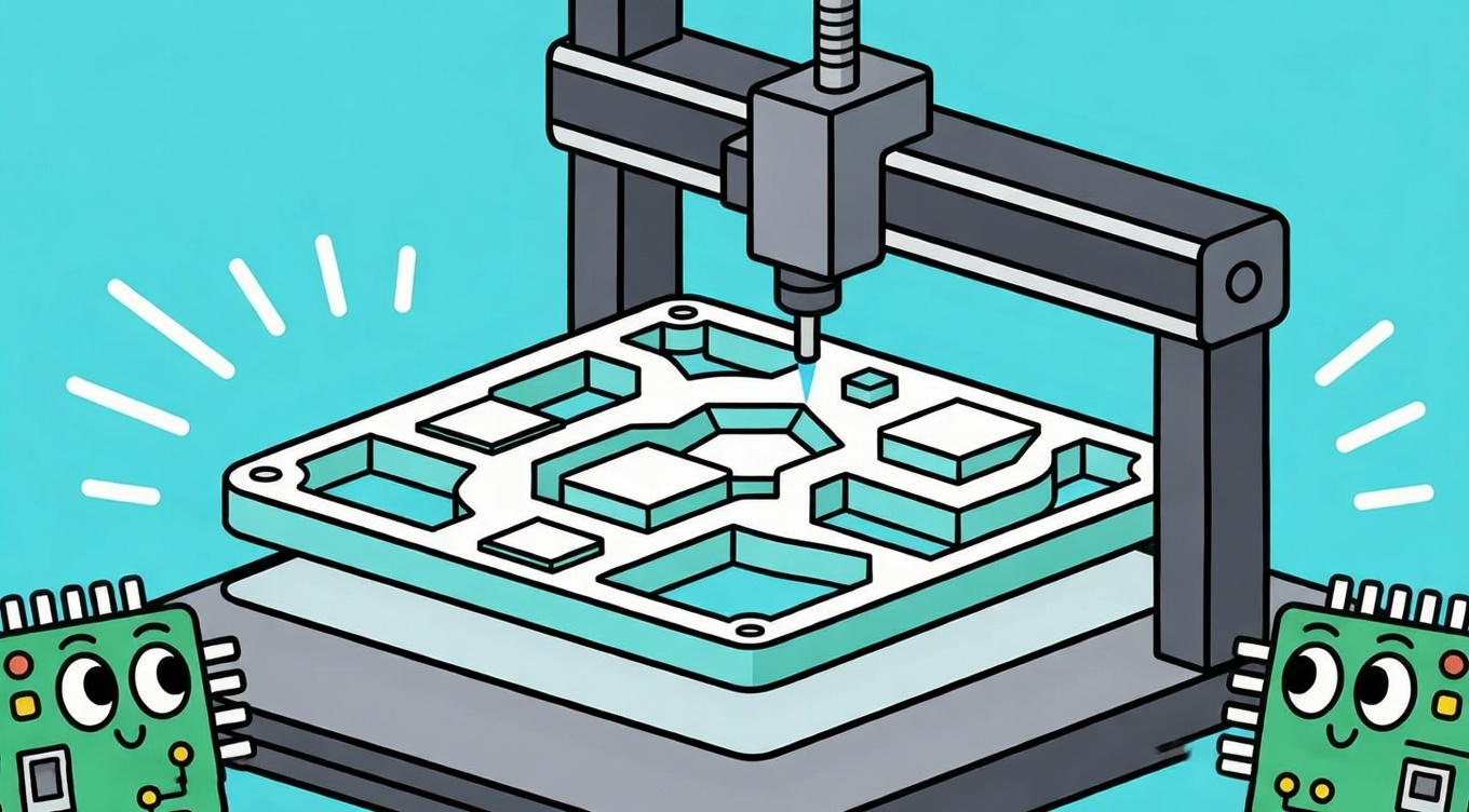
Additive manufacturing (AM) technologies are redefining how complex electronic substrates are produced — especially for ceramic PCB geometries that traditional subtractive methods struggle to fabricate. In the context of advanced electronics, complex geometries include multi-height features, embedded channels, integrated heat sinks, conformal surfaces, and 3D conductive pathways that improve performance, reliability, and integration density.
Europe, driven by stringent quality benchmarks, high technology adoption rates, and strategic electrification initiatives, is positioning additive manufacturing at the forefront of advanced ceramic PCB production by 2026. Industries such as automotive electrification, aerospace avionics, 5G infrastructure, and industrial automation increasingly demand additive solutions to meet performance targets that were unachievable with classic manufacturing.
This article walks through the technical requirements, industry standards, application drivers, design considerations, and supplier selection strategies relevant to additive manufacturing of complex ceramic PCB geometries in Europe, while outlining how BSTCERAMICPCB delivers solutions that align with European engineering expectations and quality frameworks.
The Rise of Additive Manufacturing for Complex Ceramic PCB Geometries in Europe
Additive manufacturing for ceramic PCB geometries represents a transformative approach that contrasts with traditional screen-printing, lamination, and drilling techniques. Instead of removing material, AM builds ceramic and conductive features layer by layer, enabling shapes and structures previously considered too complex or cost-prohibitive.
What Is Additive Manufacturing of Ceramic PCB Geometries?
In this context, additive manufacturing refers to techniques such as stereolithography (SLM), binder jetting, material jetting, and aerosol deposition that can deposit ceramic powder and conductive pastes with controllable resolution and repeatability. These methods allow designers to fabricate:
- Integrated cooling channels within the substrate
- Embedded antennas or waveguides for RF systems
- Variable thickness regions for thermal management
- Non-planar features suited to conformal lighting or sensor enclosures
What sets AM apart is the geometric freedom — designers are no longer confined to flat, layered fabrications but can achieve 3D substrate structures optimized for electrical and thermal performance.
Why Ceramic PCBs Need Additive Techniques for Complex Structures
Traditional ceramic PCB manufacturing excels at 2D patterns and simple multilayer stacks. However, when the design demands:
- Non-planar topologies
- Multi-height copper features
- Embedded cooling or microfluidic passages
- High aspect ratio vias with unpredictable routing
… additive manufacturing becomes a compelling alternative.
For example, in high-power modules used in automotive traction inverters or industrial drives, thermal gradients can be mitigated by additive integrated heat spreaders embedded within ceramic substrates — a feature not achievable through standard subtractive processes.
Europe’s Strategic Adoption of Ceramic PCB AM by 2026
Europe’s advanced manufacturing ecosystem — anchored in Germany, France, Sweden, and the Netherlands — is accelerating AM adoption for ceramic electronics. Public and private initiatives emphasize:
- Tech transfer from aerospace to automotive
- High-precision additive systems integrated into Industry 4.0 frameworks
- Standards harmonization to allow cross-sector supply chain alignment
In addition, European buyers evaluate AM solutions not only on geometric capability, but also repeatability, material integrity, and compliance with European and international quality frameworks (e.g., VDE, IEC, ISO).
Key Benefits of Additive Manufacturing for High-Performance Ceramic PCBs
By 2026, additive ceramic PCB geometries are expected to deliver measurable benefits:
- Improved thermal performance through internal heat channels
- Weight reduction without compromising rigidity
- Higher integration density for RF, mmWave, and power circuits
- Shorter prototyping cycles with digital design workflows
These advantages extend to sectors such as EV power electronics, high-band 5G infrastructure, avionics, and robotics — all key investment areas in Europe.

European Technical Requirements and Quality Standards for Additive Ceramic PCBs
Adoption of additive manufacturing must align with well-defined technical requirements and quality benchmarks to ensure reliability and performance.
Materials and Powder Quality for Ceramic PCB Additive Manufacturing
Material quality is the foundation of any additive ceramic PCB. Europe’s engineering teams assess:
- Particle size distribution for flow and packing density
- Purity levels to reduce dielectric defects
- Compatibility with conductive pastes (e.g., silver, copper)
Alumina (Al₂O₃) and aluminum nitride (AlN) remain dominant substrates, but when fabricating complex geometries, their behavior under sintering stresses must be predictable. Powders suitable for AM often have tighter specifications than traditional feedstocks to ensure dimensional fidelity and reduced shrinkage variability.
European standards often reference controlled sinter curves and densification thresholds measured under reproducible conditions — a critical alignment step between design expectations and production reality.
Dimensional Accuracy, Surface Finish, and Resolution Standards
Additive processes inherently influence geometric precision. European buyers expect:
- Dimensional tolerance ranges (e.g., ±50 µm or better on critical features)
- Surface roughness limits affecting solderability and assembly
- Resolution control on linewidth, via walls, and embedded features
Complex geometries require multi-axis control and feedback mechanisms (e.g., in-process optical metrology) to achieve consistent results. BSTCERAMICPCB integrates these checks to ensure that additive features meet contract specifications before downstream printing and sintering.
European Testing, Inspection, and Reliability Benchmarks
Quality engineers in Europe apply a suite of tests to validate additive parts, including:
- CT scanning for internal defect detection
- 3D surface metrology
- Thermal cycling tests per IEC or automotive standards
- Insulation resistance and breakdown voltage testing
These tests ensure substrates manufactured via AM perform reliably under operational conditions expected in automotive, aerospace, or industrial settings.
Process Control, Traceability & Certification Expectations
Traceability is a cornerstone of European quality assurance. Material batches, machine calibration records, thermal profiles, and inspection results must be traceable through digital records compliant with ISO 9001 / IATF 16949 where applicable, and documented in formats auditors expect.
BSTCERAMICPCB’s digital process control and secure trace logs facilitate compliance and customer confidence in AM ceramic PCB production.
Industry-Specific Applications and Designs Enabled by Ceramic PCB Additive Manufacturing
The value of additive ceramic PCB geometries is tied to industry-driven use cases demanding performance beyond conventional capabilities.
Automotive Electronics and Electric Power Modules
Europe’s automotive electrification wave is unparalleled. Ceramic PCBs with integrated heat spreaders, embedded coolant channels, and multi-height features offer:
- Higher power density management
- Reduced thermal gradients
- Compact packaging
AM enables designs that optimize thermal paths directly within the ceramic substrate — a leap forward for high-efficiency traction inverters and power converters.
Telecommunications, Radar, and 5G Infrastructure
5G and beyond — especially mmWave arrays — require complex RF and microstrip configurations. Additive manufacturing allows:
- Embedded waveguides
- Variable dielectric geometries
- 3D circuit paths tuned for impedance control
These advances deliver stronger signal integrity and bandwidth performance demanded by European telecom deployments.
Aerospace, Space, and Defense Electronic Subsystems
In aerospace applications, weight, reliability, and thermal control are mission-critical. AM additive ceramic substrates facilitate:
- Integrated thermal fins
- Stress-optimized structures for shock and vibration
- Reduced assembly complexity
European aerospace integrators favor additive approaches for high-reliability modules that must function across extreme environments.
Industrial Automation and High-Voltage Power Systems
Heavy industry automation, grid power electronics, and frequency converters benefit from complex ceramic PCBs that manage high currents and temperatures while integrating embedded sensors or cooling infrastructures.
Additive manufacturing accommodates intricate layouts unobtainable through planar fabrication.
Design Challenges, Tradeoffs, and Best Practices for Additive Ceramic PCB Geometries
While additive techniques unlock new possibilities, designers must balance geometric ambition with manufacturability.
Complexity vs Manufacturability vs Yield
Highly intricate features increase print time, material usage, and post-processing complexity. Yield optimization involves:
- Selecting features that benefit most from 3D geometry vs cost tradeoffs
- Strategic use of support structures
- Balancing resolution with production stability
Smarter geometries often deliver better performance with manageable complexity, preserving high production yields.
Linewidth, Via Density, and Multi-Height Features
Additive approaches allow variable linewidths and embedded via networks. However:
- Minimum printable linewidths must align with sintering shrinkage
- Dense via arrays require predictable conduction paths and thermal shrinkage compensation
- Multi-height features may impose layer sequencing constraints
BSTCERAMICPCB’s engineering teams work closely with customers to define realistic specifications that balance geometric ambition with process capability.
Hybrid AM + Subtractive Methods for Optimal Precision
In some designs, additive and subtractive processes are combined. For example:
- Additive bulk geometry
- Subtractive fine trace definition
- Polished surfaces for solderability
This hybrid strategy combines geometric sophistication with electrical precision.
Design for Manufacturability (DFM) and Simulation Practices
Simulation tools inform DFM reviews, enabling teams to predict:
- Thermal gradients
- Mechanical stress concentrations
- Dimensional deviations after sintering
Early DFM engagement accelerates development and reduces costly redesign loops.
Why European Customers Choose BSTCERAMICPCB for Additive Ceramic PCB Solutions
Engineering Collaboration and Custom AM Processes
BSTCERAMICPCB offers personalized engineering support from early design reviews through production optimization, including:
- AM process selection based on geometry and material
- Simulation-informed design adjustments
- Prototyping with performance verification
This collaborative approach de-risks innovation.
Quality Management, Inspection, and European Compliance
With digital process records, metrology systems, and traceable inspection documentation, BSTCERAMICPCB meets European expectations for:
- ISO 9001 compliant processes
- Digital reports suitable for automotive/industrial Q-audits
- Full inspection packages with shipment
Case Examples of European Additive Ceramic PCB Projects
European clients have successfully used BSTCERAMICPCB’s additive ceramic solutions for:
- Automotive power modules with embedded cooling channels
- 5G RF boards with multi-height waveguide structures
- Aerospace telemetry modules with integrated heat spreaders
These use cases validate additive methods in mission-critical systems.
Conclusion
As Europe advances into 2026 and beyond, additive manufacturing of complex ceramic PCB geometries will continue to transform how high-performance electronic substrates are designed and produced. Through improved thermal management, geometric freedom, and engineered integration, additive approaches unlock new opportunities across automotive, telecom, aerospace, and industrial sectors.
For European engineers and procurement teams seeking high-precision additive ceramic PCB solutions, BSTCERAMICPCB offers the technical depth, quality controls, and collaborative support necessary to bring innovative designs to life.
Contact us today to start your additive ceramic PCB project with confidence.
 Products
 About us
 Contact us


