


 HOME
HOME

-

AI-Driven Process Control for DPC Ceramic PCB Yield Improvement in Colombia’s Advanced Electronics Market
2026 02,28 -
Additive Manufacturing of Complex Ceramic PCB Geometries 2026 — Europe’s Technical Landscape and Industry Solutions
2026 02,27 -
Ceramic Circuit Board Quality Standards in the United States — Technical Requirements, Industry Practices, and Supplier Guide
2026 02,25 -
Ceramic PCB for LED Lighting in Colombia
2026 02,06 -
Ceramic PCB Linewidth and Line Spacing
2026 02,06 -
Ceramic PCB Development: Engineering Resilience for the UK's High-Tech Future
2026 01,30 -
Ceramic PCB for Power Modules (IGBT) in Australia — Technical Standards, Thermal Solutions, and Supplier Strategy
2026 01,23 -
Automotive-grade Aluminum Nitride Substrate in Europe — Technical Specifications, Applications, and Supplier Selection
2026 01,23 -
Ceramic PCB Solutions in Sweden: Technical Requirements, Industry Applications, and Supplier Selection Strategy
2026 01,21 -
Ceramic Substrate Custom Solutions for Poland’s High-Tech Sectors: Engineering Precision & Thermal Efficiency
2026 01,20 -
High-Temperature Resistant Ceramic PCB Solutions for Industrial LTCC and HTCC Applications
2026 01,15 -
Ceramic Circuit Board Design for the UK Electronics Industry
2026 01,13 -
BST Ceramic PCB Expands Small Batch Ceramic PCB Manufacturing Support for Swiss High-Precision Electronics
2026 01,13 -
Aluminum Nitride (AlN) Circuit Boards: Revolutionizing Thermal Management in UK Energy Storage Systems
2026 01,10 -
Top Tips for Advanced Semiconductor Packaging Substrate Design
2026 01,05 -
Automotive electronic ceramic circuits make cars smarter and safer
2026 01,05 -
The Ultimate Guide to Ceramic PCB Air Tightness: Ensuring Hermetic Reliability for High-Performance Electronics in North America
2025 12,29 -
Ceramic PCB for Power Modules (IGBT): The Ultimate High-Thermal Management Guide
2025 12,27 -
Ceramic Substrate or Aluminum PCB for High-Power LEDs
2025 12,24 -
The Ultimate Guide to Alumina Circuit Board (Al2O3): High-Performance Ceramic PCB Solutions for Global Electronics
2025 12,22 -
DBC Welding Strength Compared to Other Materials
2025 12,19 -
LTCC PCB Surprises: What Most People Miss
2025 12,09 -
Comparison of DBC PCBs and MCPCBs for Cooling Performance
2025 12,03 -
Step-by-Step Guide to DPC PCB Design for Sensor Systems
2025 12,03 -
Ceramic PCBs Essential Benefits and Applications
2025 12,01 -
How Al2O3 DPC Ceramic Substrate PCB Enhances Heat Dissipation in Modern Electronics?
2025 11,28 -
How to Choose Between Ceramic, FR4, and Metal Core PCBs
2025 11,27 -
DPC Ceramic PCB Materials: Surprising Science Inside
2025 11,26 -
Wire bondable 2-layer Alumina substrates PCB | Bstceramic PCB
2025 09,22 -
Silicon Nitride Substrate, Silicon Nitride Ceramic Substrate Formula
2025 05,08 -
How to choose the appropriate substrate for ceramic circuit boards?
2023 11,16 -
Laser Cutting or Water Saw Cutting? How To Choose the Best Cutting Solution for Ceramic Circuit Boards
2023 11,13 -
Why Ceramic PCB Is So Expensive?
2023 11,10 -
Which Process Ceramic Circuit Board Is A Better Solution For Semiconductor Refrigerator Chips?
2023 11,06 -
Silicon Printing Circuit Boards For Advancing Electronics
2023 10,27 -
What is the Difference Between HTCC and LTCC Ceramic PCB
2023 10,06 -
What is the Difference Between 96% and 99% Aluminum Oxide in Ceramic PCBs?
2023 09,20 -
Why thick film ceramic PCB is good for oil level sensor in automotive industry?
2023 08,25 -
Statistical analysis of ceramic PCB application fields
2023 08,16 -
Notice of anti-static requirements for PCBA processing and production
2023 08,16 -
Silver Paste: The Best Conductor Material for Via Holes in Thick Film Ceramic Boards
2023 08,16 -
Testing Circuit Board Ceramic Diode Fuses: A Complete Guide
2023 08,07 -
Why DBC is replaced by DPC in ceramic PCB manufacturing?
2023 08,01 -
What is thick film ceramic PCB?
2023 08,02
Ultra-High Density Design Specifications for Aluminum Nitride Ceramic Plates in Modern Electronics
Table of Contents
- Understanding Aluminum Nitride Ceramic Plates in High-Density Electronics
- U.S. Engineering Standards for Ultra-High Density Ceramic Substrate Design
- Key Structural and Thermal Design Considerations for AlN Ceramic Plates
- Application-Specific Requirements Across U.S. Industries
- Manufacturing and Inspection Strategies for Ultra-High Density Ceramic Circuits
- Why U.S. Engineers Choose BSTCERAMICPCB for Advanced AlN Substrates
Understanding Aluminum Nitride Ceramic Plates in High-Density Electronics
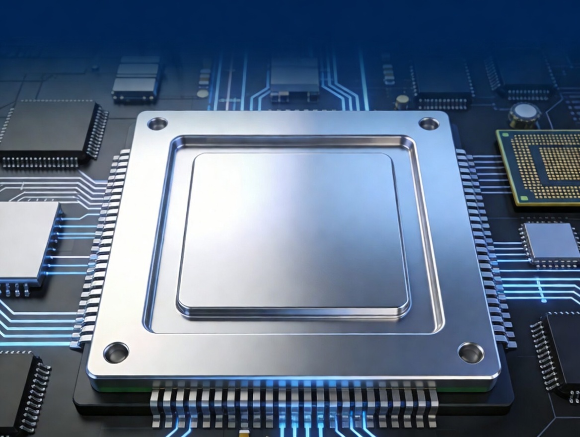
As electronic systems continue to demand higher performance, compact packaging, and superior thermal management, aluminum nitride (AlN) ceramic substrates have become a cornerstone material in advanced electronic packaging. Unlike conventional PCB materials such as FR-4, AlN ceramic plates provide a unique combination of high thermal conductivity, electrical insulation, and mechanical stability, enabling extremely dense circuit layouts without compromising reliability.
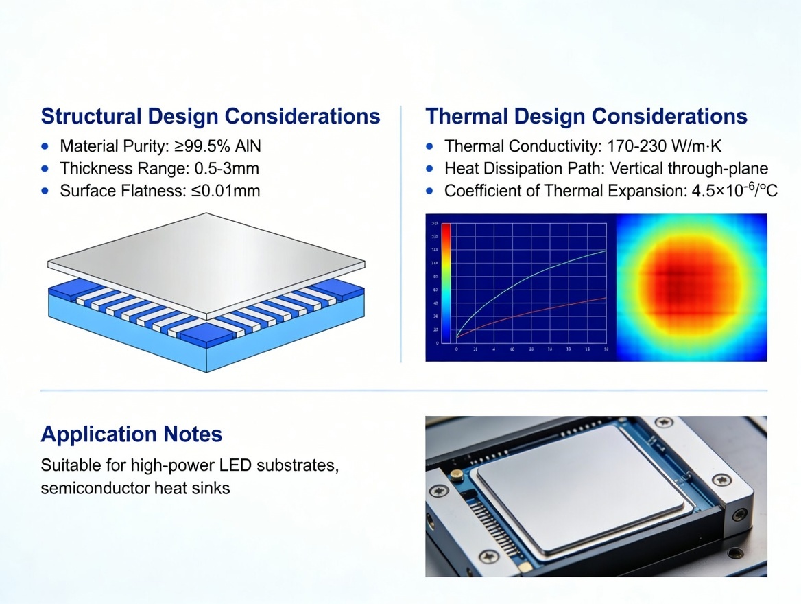
Aluminum nitride is particularly valued for its ability to conduct heat efficiently while maintaining electrical insulation. Typical AlN substrates exhibit thermal conductivity in the range of 170–220 W/m·K, far exceeding traditional ceramic materials like alumina and vastly outperforming organic PCB substrates.
This property allows heat generated by high-power semiconductor devices to be rapidly dissipated, preventing overheating and improving system lifetime. Another critical advantage is its coefficient of thermal expansion (CTE), typically around 4–6 ppm/°C, which closely matches that of silicon semiconductor devices. This compatibility minimizes thermal stress between the chip and substrate during temperature cycling, a key factor in achieving long-term reliability in high-power modules.
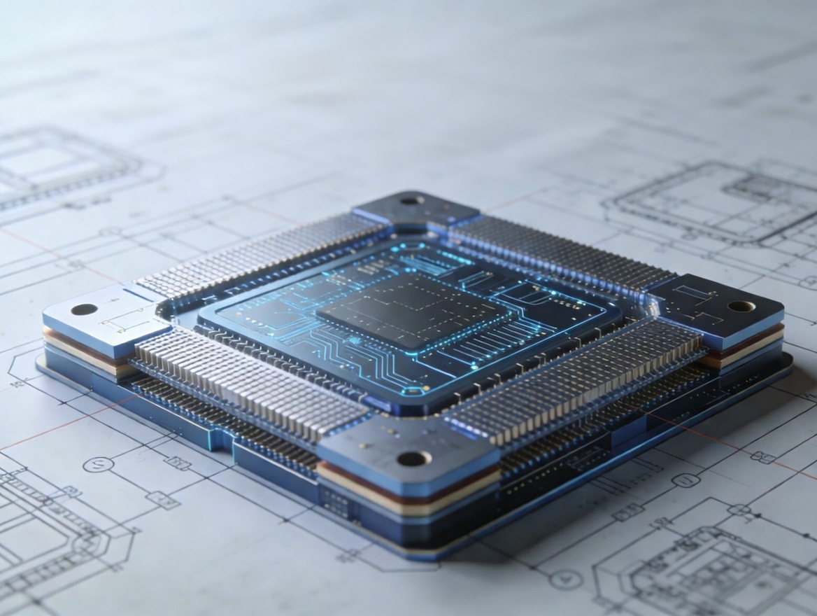
From a structural standpoint, aluminum nitride ceramic plates can support complex circuit geometries while maintaining mechanical strength. High-quality substrates may feature:
- Thermal conductivity up to 200 W/m·K
- Electrical resistivity exceeding 10¹³–10¹⁴ Ω·cm
- Flexural strength between 200–400 MPa
- Flatness tolerance below 5 μm
These properties make AlN particularly suitable for ultra-high density electronic layouts, where numerous conductive traces, vias, and semiconductor components must coexist in a limited space.
In ultra-dense electronic designs—such as GaN power modules, RF microwave circuits, or laser diode packages—the substrate must simultaneously manage:
- High current densities
- High operating temperatures
- Fine conductive patterns
- Minimal electrical noise
Aluminum nitride ceramic plates address these challenges by acting as both a thermal spreader and structural platform, allowing engineers to push the limits of device integration.
As semiconductor packaging technologies evolve toward higher power densities and miniaturized architectures, the role of ultra-high density AlN ceramic design specifications becomes increasingly critical.
U.S. Engineering Standards for Ultra-High Density Ceramic Substrate Design
In the United States, the design and qualification of ceramic substrates—including aluminum nitride plates—are governed by a combination of IPC standards, MIL-spec testing protocols, and industry-specific reliability requirements. These frameworks ensure that ceramic substrates meet strict performance benchmarks before being integrated into mission-critical systems.
The most widely referenced guideline in electronic manufacturing is the IPC classification system, which defines quality levels for electronic assemblies. For high-density ceramic substrates used in advanced electronics, designers typically target IPC Class 3, which applies to high-reliability applications such as aerospace, defense electronics, and medical devices.
Under these standards, ultra-high density ceramic plates must satisfy several design parameters.
Thermal performance criteria
The thermal management capability of the substrate must support the expected heat flux generated by semiconductor devices. Because AlN substrates offer thermal conductivity exceeding 170 W/m·K, they are commonly selected for high-power modules such as IGBT drivers, RF power amplifiers, and laser diode packages.
Thermal simulations are often required during the design stage to ensure that localized hot spots are avoided and that heat can be efficiently spread across the substrate.
Electrical insulation standards
Aluminum nitride ceramic substrates typically exhibit dielectric strengths greater than 10–20 kV/mm, ensuring reliable insulation between conductive traces even in high-voltage environments.
This characteristic allows designers to integrate densely packed circuit structures without risking dielectric breakdown.
Mechanical reliability testing
Ultra-dense ceramic designs must withstand mechanical stresses encountered during manufacturing and operation. U.S. reliability testing protocols commonly include:
- Thermal cycling tests
- Mechanical bending or flexural tests
- High-temperature operating life tests
- Environmental stress screening
These tests ensure that ceramic substrates maintain structural integrity even under extreme conditions.
Dimensional precision requirements
Ultra-high density circuits demand tight dimensional tolerances. Substrate flatness, surface roughness, and metallization thickness must be precisely controlled to support fine conductive traces and micro-vias.
As American industries continue to push the boundaries of high-performance electronics, adherence to these engineering standards ensures that ceramic substrates meet the reliability expectations of both designers and regulatory authorities.
Key Structural and Thermal Design Considerations for AlN Ceramic PCB
Designing ultra-high density circuits on aluminum nitride ceramic plates requires careful consideration of multiple engineering factors. These factors influence not only electrical performance but also manufacturability and long-term reliability.
Substrate thickness optimization
Typical aluminum nitride substrates range from 0.25 mm to 1.0 mm in thickness, depending on the required thermal capacity and mechanical stability.
Thinner substrates improve heat transfer efficiency, while thicker substrates provide increased mechanical strength.
Designers must balance these competing requirements when developing high-density modules.
Metallization structure
The metallization layer on AlN substrates can be implemented using several techniques:
- DPC (Direct Plated Copper)
- DBC (Direct Bonded Copper)
- AMB (Active Metal Brazing)
Each technology offers different advantages in terms of current capacity, pattern resolution, and mechanical reliability.
For ultra-dense layouts, thin copper layers with precise patterning capabilities are typically preferred, enabling fine trace widths and tight spacing between conductive lines.
Thermal management design
Even with excellent thermal conductivity, improper layout design can lead to localized heat buildup. Engineers must strategically distribute heat sources and incorporate thermal spreading features to maintain uniform temperature distribution.
Common strategies include:
- Copper heat-spreading planes
- Symmetrical trace layouts
- Thermal vias or heat-spreading pads
Mechanical stress control
Although aluminum nitride is mechanically strong, it remains a brittle ceramic material. Designers must account for stress generated during assembly processes such as solder reflow or die bonding.
Matching the thermal expansion properties of the substrate with those of semiconductor devices helps reduce stress concentrations and prevent cracking or delamination.
Surface finish and assembly compatibility
Surface metallization must be compatible with downstream assembly processes such as wire bonding, die attach, or soldering.
Typical finishes used on AlN ceramic plates include:
- Gold plating
- Silver metallization
- Copper plating
The correct surface finish ensures strong electrical connections and long-term reliability.
Application-Specific Requirements Across U.S. Industries
Ultra-high density aluminum nitride ceramic plates are widely used in several high-technology sectors across the United States.
Power electronics
Power electronics systems—including IGBT modules, SiC inverters, and GaN power amplifiers—generate significant heat during operation. Aluminum nitride substrates provide the thermal conductivity required to maintain safe operating temperatures.
RF and microwave systems
In RF applications such as radar modules and satellite communication systems, circuit density and signal integrity are critical. The stable dielectric constant and excellent thermal properties of AlN substrates support high-frequency operation with minimal signal loss.
Optoelectronics and laser systems
High-power laser diodes and LED arrays rely on ceramic substrates to dissipate heat efficiently. AlN ceramic plates enable compact packaging of multiple optical emitters while maintaining thermal stability.
Aerospace and defense electronics
Aerospace systems require materials capable of operating in extreme environments. Aluminum nitride’s ability to withstand high temperatures and maintain structural integrity makes it suitable for advanced avionics and sensor systems.
Semiconductor packaging
Chip carriers and advanced packaging technologies increasingly rely on ceramic substrates for thermal and electrical stability. High-density AlN substrates allow semiconductor manufacturers to integrate multiple chips within compact packages.
Manufacturing and Inspection Strategies for Ultra-High Density Ceramic Circuits
Producing ultra-high density aluminum nitride ceramic substrates requires advanced manufacturing technologies and strict quality control procedures.
Key manufacturing processes include:
- Precision ceramic sintering
- High-resolution metallization
- Laser patterning
- Advanced surface finishing
After fabrication, each substrate must undergo comprehensive inspection procedures to ensure compliance with design specifications.
Typical inspection techniques include:
- Optical inspection for surface defects
- Dimensional measurement for flatness and thickness
- Thermal conductivity testing
- Electrical insulation verification
These quality assurance processes help ensure that each ceramic substrate meets the demanding requirements of high-density electronic systems.
Why U.S. Engineers Choose BSTCERAMICPCB for Advanced Aluminum Nitride Substrates
For companies developing next-generation electronic products, selecting the right ceramic PCB manufacturing partner is essential.
BSTCERAMICPCB provides specialized expertise in the design and production of aluminum nitride ceramic plates tailored for high-density electronic applications.
Key advantages include:
- Advanced AlN ceramic PCB manufacturing capabilities
- Precision metallization technologies for dense circuit layouts
- Strict quality control and reliability testing
- Engineering support for thermal and structural optimization
BSTCERAMICPCB works closely with customers in industries such as power electronics, RF communication, and semiconductor packaging to develop ceramic substrates that meet demanding performance requirements.
By partnering with an experienced manufacturer, engineers can ensure that their ultra-high density aluminum nitride ceramic plate designs achieve optimal performance and reliability.
 Products
 About us
 Contact us


