


 HOME
HOME

-

AI-Driven Process Control for DPC Ceramic PCB Yield Improvement in Colombia’s Advanced Electronics Market
2026 02,28 -
Additive Manufacturing of Complex Ceramic PCB Geometries 2026 — Europe’s Technical Landscape and Industry Solutions
2026 02,27 -
Ceramic Circuit Board Quality Standards in the United States — Technical Requirements, Industry Practices, and Supplier Guide
2026 02,25 -
Ceramic PCB for LED Lighting in Colombia
2026 02,06 -
Ceramic PCB Linewidth and Line Spacing
2026 02,06 -
Ceramic PCB Development: Engineering Resilience for the UK's High-Tech Future
2026 01,30 -
Ceramic PCB for Power Modules (IGBT) in Australia — Technical Standards, Thermal Solutions, and Supplier Strategy
2026 01,23 -
Automotive-grade Aluminum Nitride Substrate in Europe — Technical Specifications, Applications, and Supplier Selection
2026 01,23 -
Ceramic PCB Solutions in Sweden: Technical Requirements, Industry Applications, and Supplier Selection Strategy
2026 01,21 -
Ceramic Substrate Custom Solutions for Poland’s High-Tech Sectors: Engineering Precision & Thermal Efficiency
2026 01,20 -
High-Temperature Resistant Ceramic PCB Solutions for Industrial LTCC and HTCC Applications
2026 01,15 -
Ceramic Circuit Board Design for the UK Electronics Industry
2026 01,13 -
BST Ceramic PCB Expands Small Batch Ceramic PCB Manufacturing Support for Swiss High-Precision Electronics
2026 01,13 -
Aluminum Nitride (AlN) Circuit Boards: Revolutionizing Thermal Management in UK Energy Storage Systems
2026 01,10 -
Top Tips for Advanced Semiconductor Packaging Substrate Design
2026 01,05 -
Automotive electronic ceramic circuits make cars smarter and safer
2026 01,05 -
The Ultimate Guide to Ceramic PCB Air Tightness: Ensuring Hermetic Reliability for High-Performance Electronics in North America
2025 12,29 -
Ceramic PCB for Power Modules (IGBT): The Ultimate High-Thermal Management Guide
2025 12,27 -
Ceramic Substrate or Aluminum PCB for High-Power LEDs
2025 12,24 -
The Ultimate Guide to Alumina Circuit Board (Al2O3): High-Performance Ceramic PCB Solutions for Global Electronics
2025 12,22 -
DBC Welding Strength Compared to Other Materials
2025 12,19 -
LTCC PCB Surprises: What Most People Miss
2025 12,09 -
Comparison of DBC PCBs and MCPCBs for Cooling Performance
2025 12,03 -
Step-by-Step Guide to DPC PCB Design for Sensor Systems
2025 12,03 -
Ceramic PCBs Essential Benefits and Applications
2025 12,01 -
How Al2O3 DPC Ceramic Substrate PCB Enhances Heat Dissipation in Modern Electronics?
2025 11,28 -
How to Choose Between Ceramic, FR4, and Metal Core PCBs
2025 11,27 -
DPC Ceramic PCB Materials: Surprising Science Inside
2025 11,26 -
Wire bondable 2-layer Alumina substrates PCB | Bstceramic PCB
2025 09,22 -
Silicon Nitride Substrate, Silicon Nitride Ceramic Substrate Formula
2025 05,08 -
How to choose the appropriate substrate for ceramic circuit boards?
2023 11,16 -
Laser Cutting or Water Saw Cutting? How To Choose the Best Cutting Solution for Ceramic Circuit Boards
2023 11,13 -
Why Ceramic PCB Is So Expensive?
2023 11,10 -
Which Process Ceramic Circuit Board Is A Better Solution For Semiconductor Refrigerator Chips?
2023 11,06 -
Silicon Printing Circuit Boards For Advancing Electronics
2023 10,27 -
What is the Difference Between HTCC and LTCC Ceramic PCB
2023 10,06 -
What is the Difference Between 96% and 99% Aluminum Oxide in Ceramic PCBs?
2023 09,20 -
Why thick film ceramic PCB is good for oil level sensor in automotive industry?
2023 08,25 -
Statistical analysis of ceramic PCB application fields
2023 08,16 -
Notice of anti-static requirements for PCBA processing and production
2023 08,16 -
Silver Paste: The Best Conductor Material for Via Holes in Thick Film Ceramic Boards
2023 08,16 -
Testing Circuit Board Ceramic Diode Fuses: A Complete Guide
2023 08,07 -
Why DBC is replaced by DPC in ceramic PCB manufacturing?
2023 08,01 -
What is thick film ceramic PCB?
2023 08,02
Master 3D Stackup Design for High-Power Radar Modules: A Guide for Germany's Tech Sector
Table of Contents (Quick Navigation)
- The Driving Forces Behind Germany's Demand for 3D Radar Stackups
- Critical Engineering Factors in 3D Stackup Design for High-Power Radar Modules
- Overcoming Manufacturing Bottlenecks in Multi-Layer Ceramic Substrates
- Why German Engineering Teams Trust BSTCERAMICPCB for Radar Substrates
The Driving Forces Behind Germany's Demand for 3D Radar Stackups
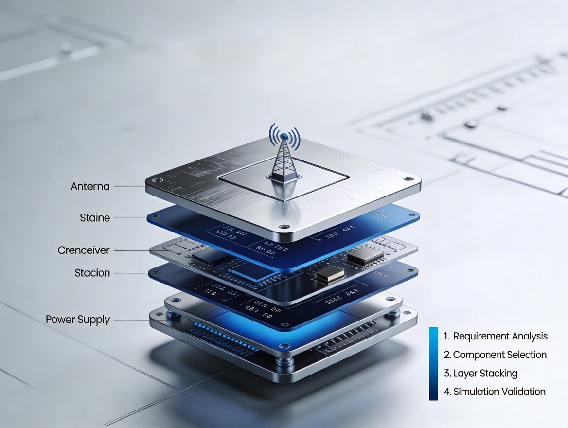
When we talk to automotive R&D directors in Stuttgart or aerospace contractors based in Bavaria, the engineering narrative is almost identical: the physical space available for electronics is shrinking, but the performance requirements are going through the roof. Germany sits at the absolute epicenter of the European transition toward autonomous driving (ADAS) and next-generation defense avionics. In both of these sectors, planar (2D) radar designs have hit a hard physical wall. You simply cannot squeeze the necessary processing power, RF transceivers, and power management units onto a single flat board without creating a catastrophic thermal nightmare or severely degrading signal integrity. This is exactly why mastering 3D stackup design for high-power radar modules is no longer an optional innovation—it is the baseline requirement for staying competitive in the German market.
Let's look at the automotive sector first. Modern vehicles require 77GHz and 79GHz millimeter-wave (mmWave) radars to achieve high-resolution imaging for features like automatic emergency braking and adaptive cruise control. These high-frequency antennas demand extremely low-loss dielectric materials. However, right beneath that antenna, you have power-hungry digital signal processors (DSPs) and transceivers generating immense heat. By moving to a 3D stackup, German engineers can vertically separate the RF antenna layers from the digital and power layers. This vertical integration drastically reduces the footprint of the radar module, allowing it to be seamlessly integrated into bumpers, side mirrors, and emblems without compromising vehicle aesthetics.
Meanwhile, Germany's aerospace and maritime sectors are pushing the boundaries of phased array radars. These systems require hundreds, sometimes thousands, of individual radiating elements packed tightly together. The power density in these active electronically scanned arrays (AESA) is staggering. Traditional PCB materials like standard FR4 or even basic PTFE blends will physically warp or melt under these conditions. A proper 3D stackup utilizes advanced ceramic materials within the layers to provide structural rigidity and a direct pathway for heat to escape. For procurement teams and design engineers navigating the strict regulatory landscape of Europe—including RoHS compliance and AEC-Q200 automotive reliability standards—finding a manufacturing partner capable of executing these complex 3D architectures is their biggest hurdle.
Critical Engineering Factors in 3D Stackup Design for High-Power Radar Modules
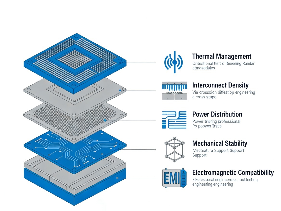
Building a multi-layer board for a low-speed consumer device is one thing; engineering a 3D stackup design for high-power radar modules is an entirely different beast. You are simultaneously managing thermophysics, electromagnetics, and mechanical stress within a block of material that might only be a few millimeters thick. When German engineering teams send us their initial Gerber files and layer stackup drafts, we immediately focus our Design for Manufacturing (DFM) review on three critical failure points.
First and foremost is thermal management. Heat is the enemy of reliability. In a 3D stackup, the heat-generating components (like power amplifiers) are often buried in the middle or bottom layers. Because heat rises and spreads, it can easily cook the sensitive RF layers sitting above them if not properly routed. We cannot rely on the substrate material alone to dissipate this. The design must incorporate dense arrays of thermal vias—specifically, copper-filled or silver-filled micro-vias—that act as microscopic exhaust pipes, channeling heat directly from the active components down to a metal core or a highly thermally conductive ceramic base layer like Aluminum Nitride (AlN). If the via placement isn't optimized, you get thermal pooling, which drastically shifts the operating frequency of the radar.
The second factor is signal integrity at millimeter-wave frequencies. At 77GHz or X-band frequencies, every tiny transition matters. When a high-speed signal jumps from layer 1 down to layer 3 through a via, that via acts as a tiny antenna itself, potentially causing impedance mismatches, signal reflections, and catastrophic insertion loss. The 3D stackup must carefully utilize ground planes and specific dielectric thicknesses to maintain exact 50-ohm impedance lines. We often have to advise our clients on the use of blind and buried vias to prevent signal stubs from radiating internal interference (crosstalk) into adjacent digital logic layers.
Finally, we have to calculate the thermomechanical stress—often referred to as CTE (Coefficient of Thermal Expansion) mismatch. A 3D radar module might include a mix of Rogers high-frequency laminates, standard bonding prepregs, and heavy copper layers. When the radar operates in a freezing German winter and then heats up rapidly to $85°C$ during operation, these materials expand at completely different rates. If the stackup isn't perfectly balanced symmetrically, the entire board will warp, snapping the fragile solder joints connecting the microchips to the board.
Overcoming Manufacturing Bottlenecks in Multi-Layer Ceramic Substrates
Understanding the physics of a 3D stackup design for high-power radar modules on a computer screen is relatively easy. Actually manufacturing it without defects is where most standard PCB houses fail completely. The German market demands perfection; a 1% failure rate in automotive ADAS systems translates to thousands of recalled vehicles. At BSTCERAMICPCB, we have spent years re-engineering our factory floor to overcome the specific bottlenecks associated with high-frequency, high-power 3D structures.
The most notorious challenge is layer-to-layer registration (alignment). When you are dealing with RF traces that are only 50 microns wide, and you need to connect them via a laser-drilled micro-via across four different layers, your alignment tolerances drop to near zero. If the layers shift by even 10 or 15 microns during the lamination pressing process, the via misses the capture pad. At radar frequencies, this misalignment doesn't just lower performance; it completely detunes the antenna array, rendering the module useless. We utilize advanced X-ray alignment systems and specialized pressing profiles to ensure that what you design in your CAD software is exactly what comes off our production line.
Another massive manufacturing hurdle is via filling and plating. To move high current and high heat out of a 3D stackup, those tiny holes connecting the layers must be completely solid. If our plating chemistry traps a microscopic air bubble inside a via (known as a void), that trapped air expands violently when the board goes through the customer's high-temperature soldering oven. The expanding gas will literally blow the via apart from the inside, a defect often called "via popping." We solve this through proprietary vacuum-assisted plating technologies, ensuring dense, void-free copper structures that can withstand extreme thermal shock.
Furthermore, integrating ceramic materials into these 3D stackups requires unique expertise. Traditional FR4 can be easily pressed together with epoxy. But combining a high-performance Alumina ($Al_2O_3$) or AlN ceramic heat spreader with softer high-frequency laminates requires complex hybrid bonding techniques. We often utilize Direct Plated Copper (DPC) technology on the ceramic layers before integrating them into the broader stackup, giving German engineers the extreme precision of thin-film circuitry combined with the brute-force heat dissipation of solid ceramic.
Why German Engineering Teams Trust BSTCERAMICPCB for Radar Substrates
The European electronics supply chain has experienced massive volatility over the past few years. German R&D teams are exhausted by long lead times, poor communication, and receiving prototypes that fail basic high-pot or thermal testing. When you are developing a cutting-edge 3D stackup design for high-power radar modules, you cannot afford to work with a broker who merely passes your files to the cheapest available factory. You need a direct manufacturing partner who speaks the language of high-frequency physics. This is why leading firms in Munich, Berlin, and Frankfurt are migrating to BSTCERAMICPCB.
We operate with total factory transparency. When you submit an inquiry to us, you are instantly connected with our CAM engineering team. We don't just quote a price; we aggressively review your 3D stackup. If we see an RF via transition that lacks a proper ground return path, or a thermal layer that risks delamination due to heavy copper imbalance, we flag it immediately. We provide actionable DFM reports before a single piece of material is cut. This proactive approach saves our German clients weeks of iterative redesigns and thousands of Euros in wasted prototype runs.
Moreover, we recognize that speed to market is everything. While traditional European suppliers might quote 6 to 8 weeks for a complex multi-layer ceramic prototype, our agile production lines are optimized for quick-turn R&D support. We can frequently deliver complex 3D radar substrate prototypes in a fraction of that time, allowing your engineering teams to validate their thermal models and RF simulations in the real world much faster.
Quality is never an afterthought; it is embedded in our culture. Every high-power radar board we produce undergoes rigorous testing. From Time Domain Reflectometry (TDR) to guarantee your 50-ohm lines are perfect, to ultrasonic scanning to ensure zero delamination between the stacked layers, we ship data alongside our boards. We handle all export logistics directly to Germany, ensuring full compliance with EU customs and environmental regulations.
Stop letting manufacturing limitations dictate your radar innovation. If your current supplier is struggling with the thermal and RF demands of your next-generation system, it’s time to upgrade your partner. Get an instant quote with your file!
 Products
 About us
 Contact us


