


 HOME
HOME

-

AI-Driven Process Control for DPC Ceramic PCB Yield Improvement in Colombia’s Advanced Electronics Market
2026 02,28 -
Additive Manufacturing of Complex Ceramic PCB Geometries 2026 — Europe’s Technical Landscape and Industry Solutions
2026 02,27 -
Ceramic Circuit Board Quality Standards in the United States — Technical Requirements, Industry Practices, and Supplier Guide
2026 02,25 -
Ceramic PCB for LED Lighting in Colombia
2026 02,06 -
Ceramic PCB Linewidth and Line Spacing
2026 02,06 -
Ceramic PCB Development: Engineering Resilience for the UK's High-Tech Future
2026 01,30 -
Ceramic PCB for Power Modules (IGBT) in Australia — Technical Standards, Thermal Solutions, and Supplier Strategy
2026 01,23 -
Automotive-grade Aluminum Nitride Substrate in Europe — Technical Specifications, Applications, and Supplier Selection
2026 01,23 -
Ceramic PCB Solutions in Sweden: Technical Requirements, Industry Applications, and Supplier Selection Strategy
2026 01,21 -
Ceramic Substrate Custom Solutions for Poland’s High-Tech Sectors: Engineering Precision & Thermal Efficiency
2026 01,20 -
High-Temperature Resistant Ceramic PCB Solutions for Industrial LTCC and HTCC Applications
2026 01,15 -
Ceramic Circuit Board Design for the UK Electronics Industry
2026 01,13 -
BST Ceramic PCB Expands Small Batch Ceramic PCB Manufacturing Support for Swiss High-Precision Electronics
2026 01,13 -
Aluminum Nitride (AlN) Circuit Boards: Revolutionizing Thermal Management in UK Energy Storage Systems
2026 01,10 -
Top Tips for Advanced Semiconductor Packaging Substrate Design
2026 01,05 -
Automotive electronic ceramic circuits make cars smarter and safer
2026 01,05 -
The Ultimate Guide to Ceramic PCB Air Tightness: Ensuring Hermetic Reliability for High-Performance Electronics in North America
2025 12,29 -
Ceramic PCB for Power Modules (IGBT): The Ultimate High-Thermal Management Guide
2025 12,27 -
Ceramic Substrate or Aluminum PCB for High-Power LEDs
2025 12,24 -
The Ultimate Guide to Alumina Circuit Board (Al2O3): High-Performance Ceramic PCB Solutions for Global Electronics
2025 12,22 -
DBC Welding Strength Compared to Other Materials
2025 12,19 -
LTCC PCB Surprises: What Most People Miss
2025 12,09 -
Comparison of DBC PCBs and MCPCBs for Cooling Performance
2025 12,03 -
Step-by-Step Guide to DPC PCB Design for Sensor Systems
2025 12,03 -
Ceramic PCBs Essential Benefits and Applications
2025 12,01 -
How Al2O3 DPC Ceramic Substrate PCB Enhances Heat Dissipation in Modern Electronics?
2025 11,28 -
How to Choose Between Ceramic, FR4, and Metal Core PCBs
2025 11,27 -
DPC Ceramic PCB Materials: Surprising Science Inside
2025 11,26 -
Wire bondable 2-layer Alumina substrates PCB | Bstceramic PCB
2025 09,22 -
Silicon Nitride Substrate, Silicon Nitride Ceramic Substrate Formula
2025 05,08 -
How to choose the appropriate substrate for ceramic circuit boards?
2023 11,16 -
Laser Cutting or Water Saw Cutting? How To Choose the Best Cutting Solution for Ceramic Circuit Boards
2023 11,13 -
Why Ceramic PCB Is So Expensive?
2023 11,10 -
Which Process Ceramic Circuit Board Is A Better Solution For Semiconductor Refrigerator Chips?
2023 11,06 -
Silicon Printing Circuit Boards For Advancing Electronics
2023 10,27 -
What is the Difference Between HTCC and LTCC Ceramic PCB
2023 10,06 -
What is the Difference Between 96% and 99% Aluminum Oxide in Ceramic PCBs?
2023 09,20 -
Why thick film ceramic PCB is good for oil level sensor in automotive industry?
2023 08,25 -
Statistical analysis of ceramic PCB application fields
2023 08,16 -
Notice of anti-static requirements for PCBA processing and production
2023 08,16 -
Silver Paste: The Best Conductor Material for Via Holes in Thick Film Ceramic Boards
2023 08,16 -
Testing Circuit Board Ceramic Diode Fuses: A Complete Guide
2023 08,07 -
Why DBC is replaced by DPC in ceramic PCB manufacturing?
2023 08,01 -
What is thick film ceramic PCB?
2023 08,02
Mastering Thermal Expansion Matching: Ceramic Plate vs. Silicon Chip for Poland’s Electronics Sector
Table of Contents
- The Critical Role of CTE Matching in Polish Power Electronics
- Ceramic Plate vs. Silicon Chip: The Physics of Thermal Expansion
- Deep Dive: Customizing Ceramic Substrates for Poland’s High-Tech Needs
- Why Polish R&D Engineers Partner with BSTCERAMICPCB
The Critical Role of CTE Matching in Polish Power Electronics
When we speak with procurement teams in Warsaw or consult with R&D engineers in Wrocław's rapidly expanding tech parks, the conversation inevitably shifts toward reliability. Poland has quietly transformed into a European powerhouse for electronics manufacturing services (EMS), particularly in the electric vehicle (EV) supply chain, renewable energy inverters, and heavy industrial automation. In these high-stakes applications, component failure isn't just an inconvenience; it represents catastrophic system downtime and massive warranty claims. At the heart of most premature electronic failures in power modules is a hidden mechanical killer: thermomechanical stress. This is precisely why understanding thermal expansion matching: ceramic plate vs. silicon chip has become the defining factor for engineering success in the Polish market.
As high-power semiconductor devices like IGBTs (Insulated-Gate Bipolar Transistors) and SiC (Silicon Carbide) MOSFETs process massive amounts of current, they generate intense, localized heat. When a device powers on, heats up, and then cools down during operation—a cycle that happens thousands of times—the materials involved physically expand and contract. If the base board expands at a drastically different rate than the semiconductor die attached to it, the solder joints connecting them experience severe shear stress. Over time, this microscopic tug-of-war leads to solder fatigue, micro-cracking, delamination, and eventually, a dead circuit.
For Polish manufacturers exporting to the broader European Union, adhering to strict automotive (like AEC-Q200) and industrial reliability standards is mandatory. Traditional FR4 printed circuit boards, while cheap, expand aggressively under heat and act as thermal insulators. They simply cannot survive the rigorous thermal cycling required by modern power electronics. Consequently, engineers are aggressively shifting toward advanced ceramic substrates. But buying just any ceramic board isn't enough; the key lies in engineering a system where the Coefficient of Thermal Expansion (CTE) of the substrate mimics that of the silicon die as closely as possible, ensuring the entire assembly "breathes" together under thermal load.
Ceramic Plate vs. Silicon Chip: The Physics of Thermal Expansion
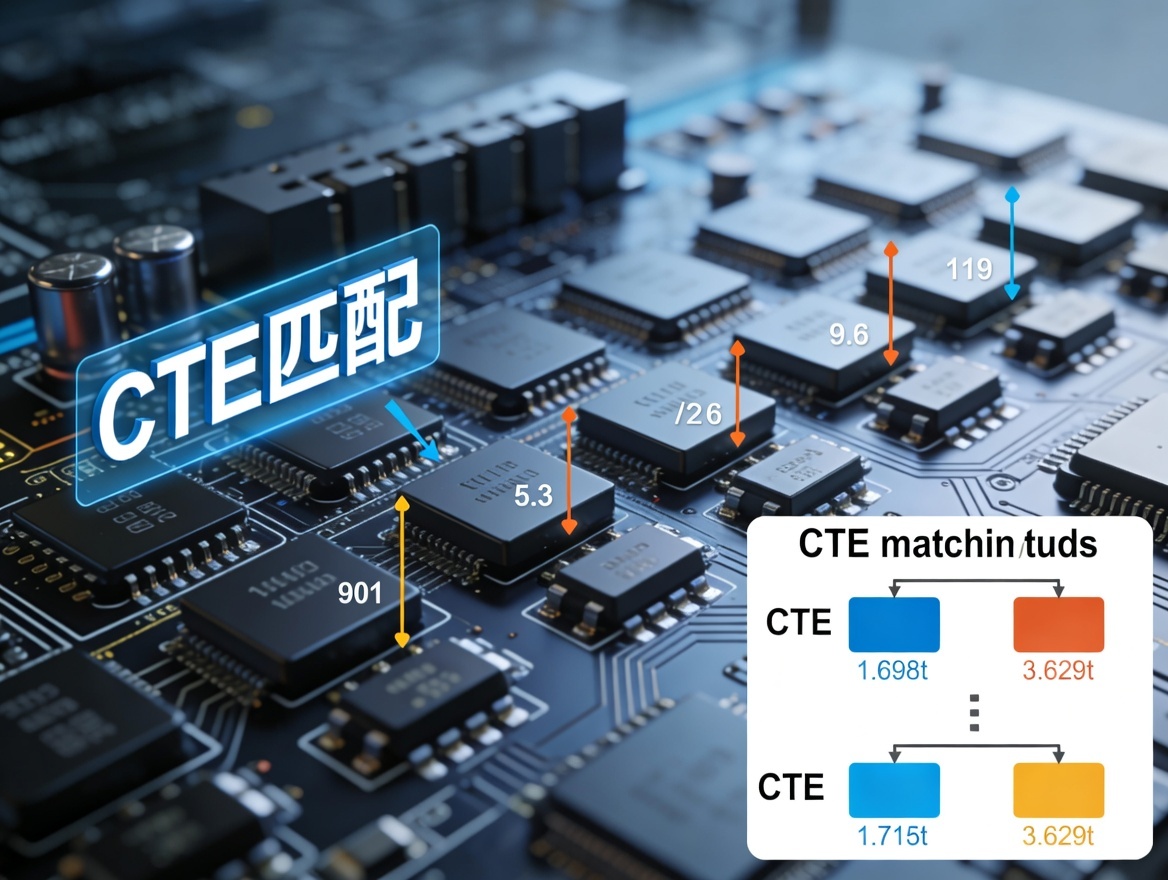
To truly grasp the dynamics of thermal expansion matching: ceramic plate vs. silicon chip, we need to look at the raw physics of the materials involved. The Coefficient of Thermal Expansion (CTE) is measured in parts per million per degree Celsius (ppm/°C). It tells us exactly how much a material stretches when its temperature rises by a single degree.
Let's start with the heart of your electronic device: the Silicon (Si) chip. Silicon has a relatively low CTE, typically hovering around 2.6 to 4.1 ppm/°C depending on the exact crystalline structure and temperature range. Now, imagine attaching this delicate, low-expansion chip directly to a standard FR4 PCB. FR4 has a CTE of roughly 14 to 17 ppm/°C. When the system heats up by 100°C during heavy operation, the FR4 board attempts to expand more than four times as much as the silicon chip sitting on top of it. The solder bumps acting as the bridge between the two are violently pulled apart. It is a textbook recipe for rapid mechanical failure.
This is where ceramic plates step in to save the day, but you have to choose the right one. The two undisputed champions in the industry are Alumina (Al2O3) and Aluminum Nitride (AlN).
- Alumina (Al2O3): Standard 96% Alumina is the industry workhorse. It offers a CTE of about 7.0 to 8.0 ppm/°C. While it doesn't match silicon perfectly, it is dramatically closer than standard PCB materials. The stress on the solder joints is reduced to a manageable level for most mid-tier power applications, making it a highly cost-effective choice for general lighting and consumer electronics.
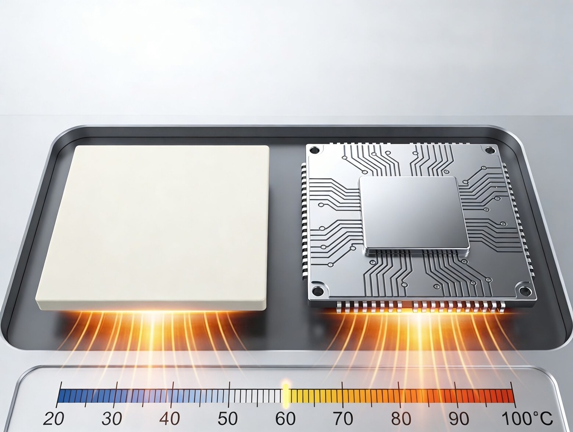
- Aluminum Nitride (AlN): For extreme power density—the kind found in Polish EV fast-charging stations and photovoltaic inverters—AlN is the ultimate material. AlN boasts a CTE of roughly 4.5 ppm/°C. This is an almost flawless match for Silicon and Silicon Carbide dies. When an AlN ceramic plate and a silicon chip heat up simultaneously, they expand in near-perfect mechanical harmony. The shear stress on the die attach interface drops to near zero. Furthermore, AlN boasts incredible thermal conductivity (up to 170-230 W/m·K), meaning it pulls heat away from the chip faster than almost any other dielectric material available.
By utilizing CTE-matched ceramics, engineers eliminate the need for bulky, unreliable thermal interface materials (TIMs) and complex mechanical compensation structures, leading to sleeker, more durable product designs that easily pass EU lifecycle testing.
Deep Dive: Customizing Ceramic Substrates for Poland’s High-Tech Needs
Recognizing the physics is only the first step; executing the design is where the real challenge lies. The Polish tech sector is highly diversified, meaning a "one-size-fits-all" approach to substrate manufacturing simply does not work. Deep ceramic substrate customization is required to bridge the gap between theoretical thermal physics and real-world assembly lines. When European engineers search for thermal expansion matching: ceramic plate vs. silicon chip, they are ultimately looking for a manufacturing partner capable of tailoring every parameter of the board to their specific module's architecture.
Here are the critical customization factors we analyze for our Polish clients:
1. Metallization Technology (DBC vs. DPC): You cannot just stick copper to a ceramic plate; it requires advanced chemical and thermal processing.
- For ultra-high current applications like EV motor drives, we customize using Direct Bonded Copper (DBC). DBC bonds thick copper foil (up to 0.3mm or more) directly to the ceramic at extreme temperatures, providing massive current-carrying capacity.
- For high-density interconnects (HDI) and miniature sensor packaging, we utilize Direct Plated Copper (DPC). DPC uses vacuum sputtering to lay down thin, highly precise copper traces (down to 50µm). We help Polish engineers select and customize the exact metallization method that balances their current load against their space constraints.
2. Dimensional and Thickness Tuning: The thickness of the ceramic base directly impacts both thermal resistance and mechanical strength. While 0.38mm and 0.635mm are standard, we routinely engineer custom thicknesses. If a Polish client is designing an aerospace component where weight is critical, we might thin the substrate. If they are building an industrial high-voltage switch, we might increase thickness to boost dielectric breakdown voltage. Furthermore, we custom-machine the outer profiles using high-precision laser routing to fit complex, non-rectangular device housings perfectly.
3. Surface Finish Requirements: Soldering compatibility is critical. To maintain the integrity of the CTE match during the assembly phase, the surface finish must be flawless. We customize finishes based on the client's assembly methods—offering ENIG (Electroless Nickel Immersion Gold) for standard reflow, ENEPIG for gold wire bonding, or Immersion Silver. We ensure every board meets the strict RoHS and REACH compliance standards mandated by the Polish and European authorities.
Why Polish R&D Engineers Partner with BSTCERAMICPCB
Understanding the delicate balance of thermal expansion matching: ceramic plate vs. silicon chip requires more than just theoretical knowledge; it demands world-class manufacturing execution. As the Polish electronics market continues to mature, moving away from low-cost assembly to high-value R&D and proprietary design, the demand for a truly capable factory partner has never been higher. This is exactly why leading European firms are bypassing local brokers and partnering directly with BSTCERAMICPCB.
First and foremost, our operation is built on engineering transparency. We are not a trading company; we own the factory floor. When a Polish engineer submits a Gerber file for a complex EV inverter substrate, our CAM engineers conduct an immediate, rigorous Design for Manufacturing (DFM) analysis. We don't blindly print what is sent to us; if we spot a trace layout that might exacerbate thermal stress points between the ceramic plate and the silicon footprint, we proactively suggest geometry modifications to ensure long-term reliability. This direct "engineer-to-engineer" communication saves our European clients weeks of trial and error.
Secondly, our quality assurance protocols are designed to validate CTE matching in the real world. Every batch of custom substrates manufactured at BSTCERAMICPCB undergoes rigorous testing. We utilize high-voltage dielectric testing, Automated Optical Inspection (AOI) to guarantee trace integrity, and thermal shock chamber testing to simulate the exact thermal cycling the boards will face in the field. We prove that the copper won't delaminate from the ceramic when the heat gets turned up.
Finally, we understand the pace of modern business. We offer rapid prototyping services specifically tailored for R&D teams, allowing Polish innovators to receive physical, highly customized ceramic samples in a fraction of the time it takes traditional suppliers. We handle the complex logistics, ensuring smooth customs clearance into the EU.
If your latest project is struggling with heat dissipation or solder joint fatigue, don't let a poorly matched substrate compromise your silicon. Contact BSTCERAMICPCB today. Let our engineering team analyze your thermal loads and deliver a custom ceramic solution that ensures your electronics outlast the competition.
 Products
 About us
 Contact us


