


 HOME
HOME

-

AI-Driven Process Control for DPC Ceramic PCB Yield Improvement in Colombia’s Advanced Electronics Market
2026 02,28 -
Additive Manufacturing of Complex Ceramic PCB Geometries 2026 — Europe’s Technical Landscape and Industry Solutions
2026 02,27 -
Ceramic Circuit Board Quality Standards in the United States — Technical Requirements, Industry Practices, and Supplier Guide
2026 02,25 -
Ceramic PCB for LED Lighting in Colombia
2026 02,06 -
Ceramic PCB Linewidth and Line Spacing
2026 02,06 -
Ceramic PCB Development: Engineering Resilience for the UK's High-Tech Future
2026 01,30 -
Ceramic PCB for Power Modules (IGBT) in Australia — Technical Standards, Thermal Solutions, and Supplier Strategy
2026 01,23 -
Automotive-grade Aluminum Nitride Substrate in Europe — Technical Specifications, Applications, and Supplier Selection
2026 01,23 -
Ceramic PCB Solutions in Sweden: Technical Requirements, Industry Applications, and Supplier Selection Strategy
2026 01,21 -
Ceramic Substrate Custom Solutions for Poland’s High-Tech Sectors: Engineering Precision & Thermal Efficiency
2026 01,20 -
High-Temperature Resistant Ceramic PCB Solutions for Industrial LTCC and HTCC Applications
2026 01,15 -
Ceramic Circuit Board Design for the UK Electronics Industry
2026 01,13 -
BST Ceramic PCB Expands Small Batch Ceramic PCB Manufacturing Support for Swiss High-Precision Electronics
2026 01,13 -
Aluminum Nitride (AlN) Circuit Boards: Revolutionizing Thermal Management in UK Energy Storage Systems
2026 01,10 -
Top Tips for Advanced Semiconductor Packaging Substrate Design
2026 01,05 -
Automotive electronic ceramic circuits make cars smarter and safer
2026 01,05 -
The Ultimate Guide to Ceramic PCB Air Tightness: Ensuring Hermetic Reliability for High-Performance Electronics in North America
2025 12,29 -
Ceramic PCB for Power Modules (IGBT): The Ultimate High-Thermal Management Guide
2025 12,27 -
Ceramic Substrate or Aluminum PCB for High-Power LEDs
2025 12,24 -
The Ultimate Guide to Alumina Circuit Board (Al2O3): High-Performance Ceramic PCB Solutions for Global Electronics
2025 12,22 -
DBC Welding Strength Compared to Other Materials
2025 12,19 -
LTCC PCB Surprises: What Most People Miss
2025 12,09 -
Comparison of DBC PCBs and MCPCBs for Cooling Performance
2025 12,03 -
Step-by-Step Guide to DPC PCB Design for Sensor Systems
2025 12,03 -
Ceramic PCBs Essential Benefits and Applications
2025 12,01 -
How Al2O3 DPC Ceramic Substrate PCB Enhances Heat Dissipation in Modern Electronics?
2025 11,28 -
How to Choose Between Ceramic, FR4, and Metal Core PCBs
2025 11,27 -
DPC Ceramic PCB Materials: Surprising Science Inside
2025 11,26 -
Wire bondable 2-layer Alumina substrates PCB | Bstceramic PCB
2025 09,22 -
Silicon Nitride Substrate, Silicon Nitride Ceramic Substrate Formula
2025 05,08 -
How to choose the appropriate substrate for ceramic circuit boards?
2023 11,16 -
Laser Cutting or Water Saw Cutting? How To Choose the Best Cutting Solution for Ceramic Circuit Boards
2023 11,13 -
Why Ceramic PCB Is So Expensive?
2023 11,10 -
Which Process Ceramic Circuit Board Is A Better Solution For Semiconductor Refrigerator Chips?
2023 11,06 -
Silicon Printing Circuit Boards For Advancing Electronics
2023 10,27 -
What is the Difference Between HTCC and LTCC Ceramic PCB
2023 10,06 -
What is the Difference Between 96% and 99% Aluminum Oxide in Ceramic PCBs?
2023 09,20 -
Why thick film ceramic PCB is good for oil level sensor in automotive industry?
2023 08,25 -
Statistical analysis of ceramic PCB application fields
2023 08,16 -
Notice of anti-static requirements for PCBA processing and production
2023 08,16 -
Silver Paste: The Best Conductor Material for Via Holes in Thick Film Ceramic Boards
2023 08,16 -
Testing Circuit Board Ceramic Diode Fuses: A Complete Guide
2023 08,07 -
Why DBC is replaced by DPC in ceramic PCB manufacturing?
2023 08,01 -
What is thick film ceramic PCB?
2023 08,02
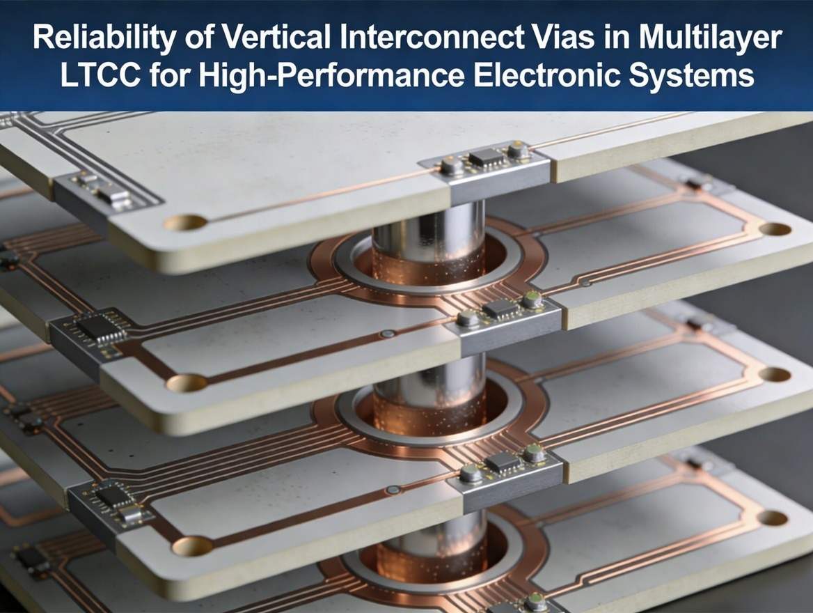
Reliability of Vertical Interconnect Vias in Multilayer LTCC for High-Performance Electronic Systems
Table of Contents
- Introduction to Vertical Interconnect Vias in Multilayer LTCC
- Engineering Standards Governing LTCC Via Reliability in the United States
- Key Failure Mechanisms Affecting LTCC Via Reliability
- Industry Applications Requiring High-Reliability LTCC Via Structures
- Design and Manufacturing Strategies to Improve LTCC Via Reliability
- Why BSTCERAMICPCB Is a Trusted LTCC Manufacturing Partner
Introduction to Vertical Interconnect Vias in Multilayer LTCC
Multilayer Low Temperature Co-fired Ceramic (LTCC) technology has become an essential packaging platform for high-frequency modules, automotive electronics, and advanced sensors. The technology allows multiple ceramic layers to be stacked, patterned with conductive traces, and co-fired into a monolithic structure. One of the most critical structural elements enabling this multilayer architecture is the vertical interconnect via, which provides electrical connectivity between stacked ceramic layers.
In LTCC manufacturing, via holes are typically formed in the green ceramic tape before firing. These holes are filled with conductive paste—commonly silver, gold, or copper—and co-fired together with the ceramic substrate. After sintering, these filled vias act as vertical conductive channels that interconnect internal circuit layers.
The reliability of these vertical vias directly influences the performance and longevity of the entire LTCC module. If a via develops micro-cracks, voids, or metallization discontinuities, electrical resistance may increase, or the interconnect may fail completely. Such failures can cause signal loss, thermal hotspots, or system malfunction in mission-critical electronics.
In high-density multilayer LTCC modules, hundreds or even thousands of vertical vias may be integrated into a single substrate. Typical LTCC design rules indicate via diameters in the range of 0.004–0.008 inches, depending on process capability, with corresponding pad and spacing requirements.
For German industries that rely heavily on precision electronics—such as automotive power electronics, telecommunications infrastructure, and industrial automation—via reliability is not simply a manufacturing metric but a crucial quality indicator. These industries demand long-term operational stability under conditions such as:
- High temperature cycling
- Mechanical stress
- High-frequency signal transmission
- Harsh industrial environments
To meet these expectations, manufacturers must carefully control the materials, processing conditions, and inspection techniques used during LTCC production. In practice, achieving reliable via structures requires close coordination between circuit designers, materials engineers, and ceramic PCB manufacturers.
Engineering Standards Governing LTCC Via Reliability in the United States
Although the target market for this article is Germany, many of the engineering practices used in European electronics manufacturing are derived from U.S. reliability standards and international IPC specifications. These frameworks define the testing procedures and structural benchmarks required to ensure that multilayer ceramic substrates maintain electrical integrity throughout their operational life.
One of the most widely referenced frameworks is the IPC reliability classification system, which categorizes electronic assemblies based on their required reliability levels. For example:
- IPC Class 2 applies to standard consumer electronics.
- IPC Class 3 is designed for high-reliability equipment such as aerospace, medical devices, and automotive control systems.
For LTCC modules used in safety-critical applications, most manufacturers target Class 3 workmanship and reliability requirements.
Under these standards, several parameters are evaluated when assessing via reliability:
Material compatibility
The ceramic substrate and the conductive paste used for vias must exhibit compatible sintering shrinkage behavior. Differences in shrinkage between the ceramic body and the conductive metallization can cause mechanical stress during firing, potentially leading to delamination or warping.
Thermal expansion matching
The coefficient of thermal expansion (CTE) of LTCC materials typically falls around 5–6 ppm/°C, which must align with the metals used in the vias to prevent stress accumulation during temperature cycling.
Electrical and mechanical testing
Standard reliability verification procedures include:
- Thermal shock testing
- High-temperature storage
- Humidity bias testing
- Mechanical pull testing
- Electrical continuity inspection
Manufacturers often combine these tests with advanced inspection techniques such as automated optical inspection (AOI) and X-ray imaging to detect voids or incomplete metallization within the vias.
For German electronics manufacturers supplying the automotive and telecom sectors, adherence to these standards ensures that LTCC substrates can operate reliably for many years without degradation.
Key Failure Mechanisms Affecting LTCC Via Reliability
Despite the inherent stability of ceramic materials, several failure mechanisms can compromise the reliability of vertical vias in multilayer LTCC structures.
Sintering mismatch
During co-firing, the ceramic layers and the conductive paste undergo shrinkage as the materials densify. If the shrinkage rates differ significantly, internal stress can develop, leading to cracks around the via interface. This mismatch is one of the most common reliability challenges in LTCC manufacturing.
Void formation
Incomplete filling of via holes with conductive paste can produce voids or air pockets inside the interconnect. These voids increase electrical resistance and reduce the ability of the via to conduct heat.
Delamination between layers
In multilayer structures, insufficient lamination pressure or contamination during stacking can cause layers to separate during firing. When delamination occurs near via structures, the electrical connection between layers may be compromised.
Thermal fatigue
Repeated temperature cycling can gradually weaken the metallurgical interface between the via conductor and the surrounding ceramic material. Over time, this can result in micro-cracks and eventual open circuits.
Electrical overstress
High-power electronics applications may subject vias to significant current density. If the via diameter or metallization thickness is insufficient, localized heating may accelerate degradation.
Understanding these failure mechanisms is essential for designers and manufacturers seeking to develop LTCC substrates capable of meeting the stringent reliability expectations of the German electronics market.
Industry Applications Requiring High-Reliability LTCC Via Structures
Multilayer LTCC technology is widely used in applications where compact integration, high-frequency performance, and environmental stability are required.
Automotive electronics
Modern vehicles integrate numerous electronic control units, radar sensors, and power modules. LTCC substrates are commonly used in automotive radar systems and power electronics due to their excellent thermal stability and electrical insulation properties.
For these applications, via reliability is critical because failures can affect safety-related systems such as advanced driver-assistance systems (ADAS).
Telecommunications infrastructure
5G base stations and RF modules often rely on LTCC substrates to integrate passive components and high-frequency circuits within compact packages. LTCC technology supports high-frequency operation with low dielectric loss, making it ideal for RF applications.
Industrial automation
Germany’s manufacturing sector depends heavily on industrial control systems and sensor networks. These systems must operate reliably in harsh environments that may involve vibration, humidity, and wide temperature ranges.
Aerospace and defense electronics
Although not always publicly documented, LTCC substrates are frequently used in aerospace electronics due to their mechanical strength and ability to withstand extreme environmental conditions.
Design and Manufacturing Strategies to Improve LTCC Via Reliability
To achieve consistent via reliability in multilayer LTCC substrates, manufacturers must optimize both the design and production stages.
Via geometry optimization
Designers must carefully select via diameter, aspect ratio, and spacing to ensure proper paste filling and mechanical stability. Extremely small vias may increase integration density but also raise the risk of incomplete metallization.
Controlled lamination processes
Proper lamination pressure and temperature ensure that the stacked ceramic layers bond uniformly before firing, preventing layer separation.
Advanced inspection techniques
Modern LTCC production lines employ a variety of inspection technologies:
- X-ray inspection
- Optical scanning systems
- Automated optical inspection (AOI)
These techniques allow manufacturers to identify defects early in the production process.
Process parameter control
Precise control of firing temperature, atmosphere, and dwell time ensures uniform sintering of the ceramic layers and conductive materials.
By combining these strategies, manufacturers can significantly improve the yield and long-term reliability of LTCC via structures.
Why BSTCERAMICPCB Is a Reliable LTCC Manufacturing Partner
For companies developing advanced electronic modules for the European market, selecting the right LTCC manufacturing partner is critical.
BSTCERAMICPCB provides comprehensive ceramic PCB manufacturing services, including LTCC multilayer substrates designed for high-reliability applications. The company’s production processes are optimized to maintain consistent via integrity and dimensional accuracy.
Key capabilities include:
- Advanced multilayer LTCC fabrication
- Precision via drilling and metallization
- Controlled lamination and co-firing processes20
- Comprehensive electrical and mechanical testing
These capabilities enable BSTCERAMICPCB to support industries such as automotive electronics, telecommunications, and industrial automation with reliable ceramic PCB solutions.
For engineers seeking to improve the reliability of vertical interconnect vias in multilayer LTCC substrates, collaborating with an experienced manufacturing partner can significantly reduce development risks and accelerate time-to-market.

To learn more about LTCC design and manufacturing capabilities, visit:
 Products
 About us
 Contact us


